In this post, we continue our deep dive comparison of the security processors used on a consumer product and an unlicensed clone. Our focus here will be comparing manufacturing process technology.
We already know the sizes of both dies, so given the gate density (which can be roughly estimated from the technology node or measured directly by locating and measuring a 2-input NAND gate) it’s possible to get a rough estimate for gate count. This, as well as the number of metal layers, can be used as metrics for overall device complexity and thus difficulty of reverse engineering.
For a more accurate view of device complexity, we can perform some preliminary floorplan analysis of each device and estimate the portions of die area occupied by:
Analog logic (generally uninteresting)
Digital logic (useful for gate count estimates)
RAM (generally uninteresting aside from estimating total bit capacity)
ROM/flash (allows estimating capacity and, potentially, difficulty of extraction)
OEM Component
We’ll start with the OEM secure element and take a few cross sections using our dual-beam scanning electron microscope/focused ion beam (SEM/FIB). This instrument provides imaging, material removal, and material deposition capabilities at the nanoscale.
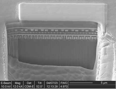
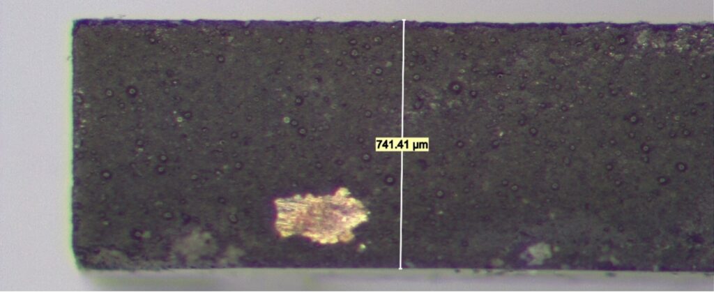
Figure 1. SEM image showing FIB cross section of OEM component
To cross section a device, the analyst begins by using deposition gases to create a protective metal cap over the top of the region of interest. This protects the top surface from damage or contamination during the sectioning process. This is then followed by using the ion beam to make a rough cut a short distance away from the region of interest, then a finer cut to the exact location. The sample can then be imaged using the electron beam.
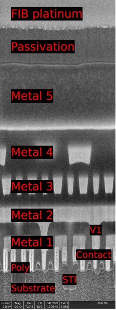
Figure 1 shows a large rectangular hole cut into the specimen, with the platinum cap at top center protecting the surface. Looking at the cut face, many layers of the device are visible. Upon closer inspection (Figure 2), we can see that this device has four copper interconnect layers followed by a fifth layer of aluminum.
At higher magnification (Figure 3), we can clearly see individual transistors. The silicon substrate of the device (bottom) has been etched to enhance contrast, giving it a rough appearance. The polysilicon transistor gates, seen end-on, appear as squares sitting on the substrate. The bright white pillars between the gates are tungsten contacts, connecting the source and drain terminals of each transistor to the copper interconnect above.
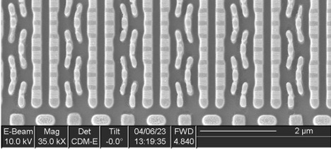
Figure 4. 6T SRAM bit cells on OEM component
Based on measurements of the gates, we conclude that this device is made on a 90 nm technology:
Contacted gate pitch: 282 nm
M1 pitch: 277 nm
6T SRAM bit cell (Figure 4): 1470 x 660 nm (0.97 µm2)
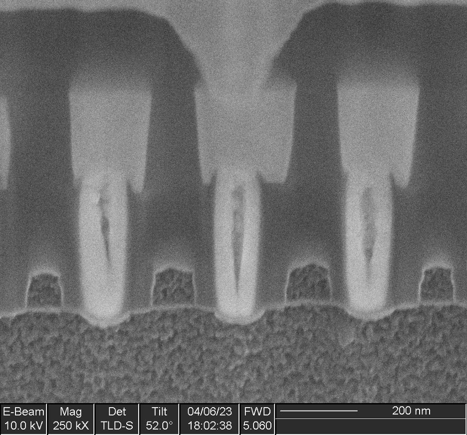
We can also use cross sections to distinguish between various types of memory. Figure 5 is a cross section of one of the memory arrays of the OEM device, showing a distinctive double-layered structure instead of the single polysilicon gates seen in Figure 3. This is a “floating gate” nonvolatile memory element; the upper control gate is energized to select the cell while the lower floating gate stores charge, representing a single bit of memory data.
The presence of metal contacts at both sides of each floating gate transistor (rather than at either end of a string of many bits) allows us to complete the classification of this memory as NOR flash, rather than NAND.
Figure 5. Cross section of NOR flash memory on OEM component showing floating gates
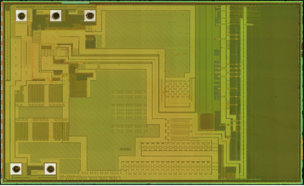
The overall device is approximately 2400 x 1425 µm (3.42 mm2), broken down as:
67% (2.29 mm2): memories and analog IP blocks
33% (1.13 mm2): standard cell digital logic
Multiplying the logic area by an average of published cell library density figures for the 90nm node results in an estimated 475K gates of digital logic (assuming 100% density) for the OEM security processor. The actual gate count will be less than this estimate as there are some dummy/filler cells in less dense areas of the device.
Clone Component
Performing a similar analysis on the clone secure element, we see five copper and one aluminum metal layers (Figure 6).
Figure 6. Cross section of clone security processor showing layers
Figure 7. Closeup of SRAM transistors from clone security processor
Interestingly, the clone secure element is made on a more modern process node than the OEM component:
Contacted gate pitch: 225 nm
Minimum poly pitch: 158 nm
SRAM bit cell: 950 x 465 nm (0.45 µm2)
The transistor gates appear to still be polysilicon rather than metal.
Figure 8. NAND2 cell from clone component, substrate view with metal and polysilicon removed
These values are in-between those reported for the 65 nm and 45 nm nodes, suggesting this device is made on a 55 nm technology. The lack of metal gates (which many foundries began using at the 45 nm node) further reinforces this conclusion.
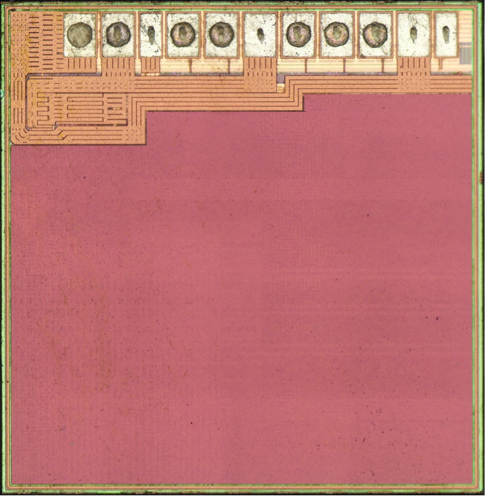
The overall device is approximately 1190 x 1150 µm (1.36 mm2), broken down as:
37% (0.50 mm2): memories
27% (0.36 mm2): analog blocks and bond pads
31% (0.42 mm2): standard cell digital logic
5% (0.07 mm2): filler cells, seal ring, and other non-functional areas
Given the roughly 0.42 mm2 of logic and measured NAND2 cell size of 717 x 1280 nm (0.92 µm2 or 1.08M gates/mm2 at 100% utilization), we estimate a total gate count of no more than 450K—slightly smaller than the OEM secure element. The actual number is likely quite a bit less than this, as a significant percentage (higher than on the OEM part) of the logic area is occupied by dummy/filler cells.
In part 3, we continue our deep dive comparison of the security processors used on a consumer product and an unlicensed clone. There we will focus on identifying and characterizing the memory arrays.
Manufacturers of consumer electronics often use embedded security processors to authenticate peripherals, accessories, and consumables. Third parties wishing to build unlicensed products (clones) within such an ecosystem must defeat or bypass this security for their products to function correctly.
In this series, the IOActive silicon lab team will take you on a deep dive into one such product, examining both the OEM product and the clone in detail.
Fundamentally, the goal of a third party selling an unlicensed product is for the host system to recognize their product as authentic. This can be achieved by extracting key material from an OEM or licensed accessory and putting it on a new processor (difficult, but allows the third party to manufacture of an unlimited number of clones) or by recycling security processors from damaged or discarded accessories (low effort since there is no need to defeat protections on the secure element, but the number of clones is limited by the number of security chips that the third party can find and recycle). In some cases, it may also be possible to bypass the cryptographic authentication entirely by exploiting implementation or protocol bugs in the authentication handshake.
We’ll begin our analysis by comparing the security processors from an OEM and clone device to see which path was taken in this case. The first step is to locate the processors, which can be challenging since security chips tend to have deliberately confusing or nondescript markings to frustrate reverse-engineering efforts.
Package Comparison
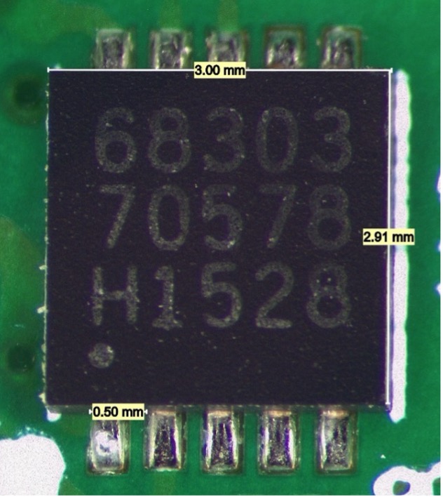
Figure 1. Security processor from OEM device
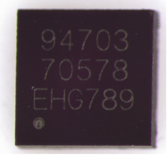
Figure 2. Security processor from clone device
Comparing the top-side markings, we see:
The first three digits of the first line are different.
The second line is identical.
The third line is completely different: three letters and three numbers on the clone versus one letter and four numbers on the OEM part.
The font weight of the laser engraving is lighter on the clone and heavier on the OEM.
There is no manufacturer logo marked on either device.
The pin 1 marking dot of the OEM part has a well-defined edge, while the pin 1 marker of the clone has a small ring of discoloration around it.
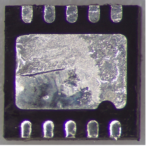
Both components are packaged in an 8-pin 0.5 mm pitch DFN with a thermal pad featuring a notch at pin 1 position. No distinction is visible between the devices from the underside.
Figure 3. Underside of clone component
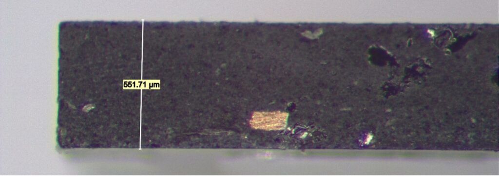
Looking from the side, we see that the clone package is significantly thicker.
Figure 4. Side view of OEM component
Figure 5. Side view of clone component
Top Metal Comparison
At this stage of the analysis, it seems likely that the devices are different given the packaging variations, but this isn’t certain. Semiconductor vendors occasionally change packaging suppliers or use multiple factories to improve supply chain robustness, so it’s entirely possible that these components contain the same die but were packaged at different facilities. In order to tell for sure, we need to depackage them and compare the actual silicon.
After depackaging, the difference is obvious, even before putting the samples under the microscope. The OEM die is rectangular and about 2.6x the area of the clone die (3.24 mm2 for the OEM versus 1.28 mm2 for the clone). It also has a yellow-green tint to it, while the clone is pink.
Figure 6. Top metal image of OEM die
Figure 7. Top metal image of clone die
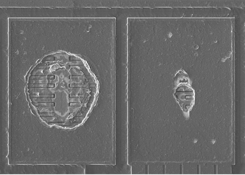
The OEM die has five gold ball bonds, three in the top left and two in the bottom left.
In contrast, the clone die has 11 pads along the top edge. Two are narrower than the rest and appear intended for factory test only, two redundant power/ground pads are full sized but unbonded (showing only probe scrub marks from factory test), and the remaining seven have indentations from copper ball bonds (which were chemically removed to leave a flat specimen surface).
Figure 8. Used bond pad on clone die (left, bond ball removed) vs. unused pad (right, showing probe mark)
The OEM die has no evidence of an antitamper mesh; however, the surface appears to be completely covered by a dense grid of power/ground lines in-between larger high-current power distribution buses. The only exception is the far-right side, which is only covered by CMP filler (dummy metal features serving no electrical function, but which aid in manufacturability). Since sensitive data lines are not exposed on the top layer, the device is still protected against basic invasive attacks.
The clone die has large power and ground distribution buses on the top edge near the bond pads, while the remainder of the surface is covered by a fine mesh of wires clearly intended to provide tamper resistance. Typically, secure elements will fail to boot and/or erase flash if any of these lines are cut or shorted while the device is under power.
Figure 9. Antitamper mesh on the clone die
Neither die has any vendor logo or obvious identifying markings on it. The OEM part has no markings whatsoever; the clone part has mask revision markings suggesting six metal layers and a nine-digit alphanumeric ID code “CID1801AA” (which returned no hits in an Internet search).
Figure 10. Die markings on clone secure processor
Concluding Thoughts
The clone security processor is clearly a different device from the OEM part rather than a recycled chip. This means that the third party behind the clone must have obtained the authentication key somehow and flashed it to their own security processor.
Interestingly, the clone processor is also a secure element with obvious antitamper features! We believe that the most likely rationale is that the third party is attempting to stifle further competition in the market—they already have to share the market with the OEM but are trying to avoid additional clones becoming available.
The clone part also looks very similar to the OEM part upon casual inspection—both are packaged in the same 8-pin DFN form factor and have markings that closely resemble one another. Normally this is a sign of a counterfeit device; however, there is little chance of the OEM buying their security chip from an untrustworthy source, so it seems doubtful that the clone chip manufacturer was intending to fool the OEM into using their part. One possible explanation is that the authentication scheme was defeated by a fourth party, not the manufacturer of the clone accessory, and that they produced this device as a drop-in equivalent to the OEM security processor to simplify design of clones. Using a footprint compatible package and marking it with the same ID number would make sense in this scenario.
In the next part of this series, we’ll compare the manufacturing process technology used on the two components.
Hack the Sky: Adventures in Drone Security | Gabriel Gonzalez
By
Gabriel Gonzalez
Taking aim at the attack surface of these buzzy devices uncovers real-world risks
In the grand theater of innovation, drones have their spot in the conversation near the top of a short list of real game changers, captivating multiple industries with their potential. From advanced military applications to futuristic automated delivery systems, from agricultural management to oil and gas exploration and beyond, drones appear to be here to stay. If so, it’s time we start thinking about the security of these complex pieces of airborne technology.
The Imperative Around Drone Security
Now, I know what you’re thinking. “Drone security? Really? Isn’t that a bit… extra?”
Picture this: A drone buzzing high above a bustling city, capturing breathtaking views, delivering packages, or perhaps something with more gravitas, like assisting in life-saving operations. Now, imagine that same drone spiraling out of control, crashing into buildings, menacing pedestrians — or worse, being used as a weapon.
Drone security isn’t just about keeping flybots from crashing into your living room. It’s about ensuring that these devices, which are increasingly a part of our everyday lives, are hardened against the actions of those with malicious intent. It’s about understanding that while drones can be used for good, they can also be used for nefarious purposes.
And BTW, hacking a drone remotely is just plain cool.
But let’s not get carried away. While the idea of hacking a drone might sound like something out of a spy movie, it’s a very real threat. And it’s a threat that we need to take seriously. Let’s dive a little deeper.
Drones: The Other Kind of Cloud Vulnerabilities
Before we delve into the nitty-gritty of drone hacking, let’s take a moment to understand them. Drones are either controlled remotely or they fly autonomously through software-controlled flight plans embedded in their systems working in conjunction with onboard sensors and the satellite-based Global Positioning System (GPS).
At the heart of a drone’s operation — and the bullseye for any security research — is its firmware and its associated microcontroller or CPU. This is the software/chip combination that controls the drone’s flight and functionality. It’s the drone’s brain. And just like any brain, we’re sorry to report, it has weaknesses.
Drones, like any other piece of technology, are not impervious to attack. They present us with a few attack surfaces – the backend, mobile apps, RF communication, and the physical device itself.
Electromagnetic (EM) Signal: A Powerful Tool for Hacking
Now that we’ve covered the basics let’s move on to the star of the show – the Electromagnetic (EM) signal. EM signals are essentially waves of electric and magnetic energy moving through space. They’re all around us, invisible to the naked eye but controlling much of our daily life.
These pulses can be used to interfere with the way a drone “thinks”, creating unexpected bad behavior in the core processor, disrupting its operations, or pushing the onboard controller to reveal information about itself and its configurations. It’s like having a magic wand that can bypass all the security systems, influence critical systems behavior, and even potentially take control of the drone. Sounds exciting, doesn’t it?
The potential of EM signals to bypass drone security systems is a concern and a threat that needs to be addressed quickly.
Case Study: Hacking a Drone with EM Fault Injection
Let’s walk through our real-world example of a drone being hacked using EM signals.
In this particular IOActive research, we used EM signals to interfere with the drone’s functionality by disrupting the routine processing of the device’s “neural activity” in its core microprocessor “brain” and branching out to its various onboard peripheral systems.
Most people are familiar with Electroencephalography (EEG) and Deep Brain Stimulation (DBS) — using electrodes and electrical impulses to both monitor and influence activity in the human brain. Our approach here is analogous to that, but with fewer good intentions and at a much greater distance.
Our initial strategy involved attempting to retrieve the encryption key using EM emanations and decrypting the firmware. We began by locating an area on the drone’s PCB with a potent EM signal to place a probe and record sufficient traces to extract the key.
After identifying the location with the strongest signal, we worked on understanding how to bypass the signature verification that takes place before the firmware is decrypted.
After several days of testing and data analysis, we found that the probability of a successful signature bypass was less than 0.5%. This rendered key recovery unfeasible since it would have required us to collect tens of thousands of traces.
Our subsequent — and more fruitful — strategy involved using ElectroMagnetic Fault Injection (EMFI), inspired by ideas published by Riscure. With EMFI, a controlled fault can be used to transform one instruction into another, thereby gaining control of, say, the PC register. We can generate an EM field strong enough to induce changes within the “live bytes” of the chip. It’s very much like sending DBS current to the human brain and getting the muscles to behave in an unconscious, uncontrolled way.
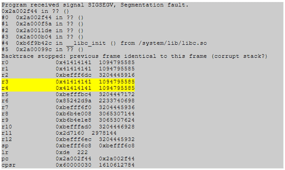
After identifying a small enough area on the PCB, we tweaked the glitch’s shape and timing until we observed a successful result. The targeted process crashed, as shown here:
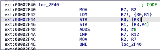
Our payload appeared in several registers. After examining the code at the target address, we determined that we had hit a winning combination of timing, position, and glitch shape. This capture shows the instruction where a segmentation error took place:
Having successfully caused memory corruption, the next step would be to design a proper payload that achieves code execution. An attacker could use such an exploit to fully control one device, leak all of its sensitive content, enable access to the Android Debug Bridge, and potentially leak the device’s encryption keys.
Drone Security: Beyond the Horizon
So, where does this leave us? What’s the future of drone security?
The current state of drone defenses is a mixed bag. On one hand, we have advanced security systems designed to protect drones from attacks. On the other hand, we have researchers — like us — constantly scheming new ways to bypass such systems.
The future of drone cyber-protections lies in ongoing research and development. We must stay one step ahead and identify weaknesses so manufacturers can address them. This post is just a summary of a much longer research paper on the topic; I encourage you to check out the full report.
Follow along with us at IOActive to keep up with the latest advancements in the field, understand the threats, and take action. The sky is not just the limit. It’s also a battlefield, and we need to be prepared.
In our previous post on platform security (see here) we provided a brief introduction into platform security protections on AMD-based platforms and touched upon the topic of AMD Platform Secure Boot (PSB).
As a quick reminder, the purpose of PSB is to provide a hardware root-of-trust that will verify the integrity of the initial UEFI firmware phases, thereby preventing persistent firmware implants.
In this part of the blog series, we will dig deeper into the nitty gritty details of PSB, including a first glimpse of how it works under the hood, how it should be configured and, naturally, how various major vendors fail to do so.
Architecture
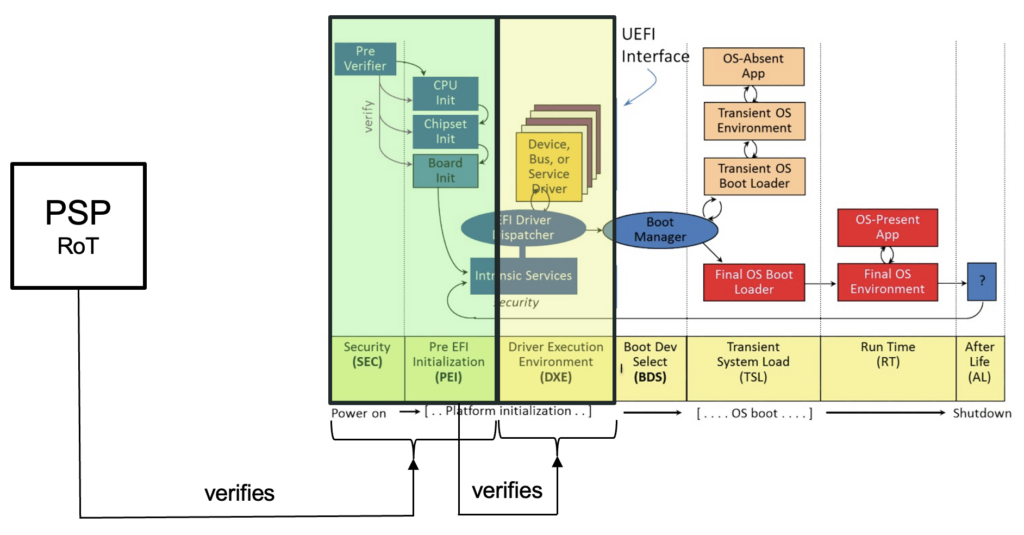
To begin, it is important to understand that the UEFI boot process is divided into various phases, referred to as SEC, PEI, DXE, BDS, TSL, RT and AL. For the sake of brevity, we won’t go into detail on the purpose of each phase as it has already been widely covered already (e.g. here).
In short, the role of the PSB is to ensure that the initial UEFI phases, specifically the SEC and PEI phase, are properly verified and cannot be tampered with. In turn, the PEI phase will verify the DXE phase using a proprietary and vendor-specific method.
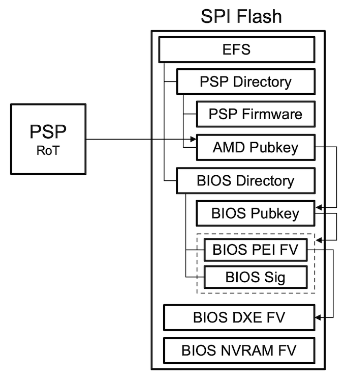
The resulting scheme is summarized in the following image:
Upon reset, only the AMD Platform Security Processor (PSP), an ARM-based co-processor embedded within the AMD chip, is running. It functions as a hardware root-of-trust and verifies the SEC and PEI phase portions of the UEFI firmware. If verification succeeds, then it releases the main cores that then start executing the SEC and PEI phase.
Trust Hierarchy
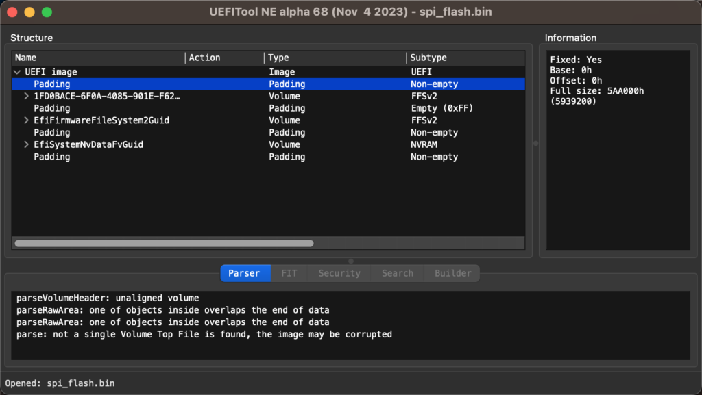
In order to understand the trust hierarchy in more depth, we will first take a look at how the UEFI firmware, stored in the SPI flash, is structured. To do so, we will use the SPI flash dump we have obtained from an AMD-based Huawei Matebook 16 (BIOS v2.28).
When we open up a SPI flash dump with our trusty UEFI Tool, we will typically see, among others, the following structures:
Padding areas
Firmware volumes (containing DXE drivers and SMM modules)
NVRAM data (containing non-volatile configuration data, i.e. UEFI variables)
However, while UEFI Tool correctly identifies firmware volumes that contain code executed in the DXE phase of the UEFI boot process, the code running in the SEC and PEI phases seems to be missing altogether.
This is because it does not support parsing an AMD platform specific structure called the Embedded Firmware Structure (EFS). Once again, for the sake of brevity, as the structure is relatively complex, we will only focus on portions relevant to the chain-of-trust.
As described here, the EFS is located at one of the pre-defined locations in the SPI flash and contains pointers to:
The PSP directory table that includes:
The BIOS signing key (entry type 0x05)
The BIOS PEI firmware volume (entry type 0x62)
The BIOS PEI firmware volume signature (entry type 0x07)
The BIOS directory table that includes:
The AMD root signing key (entry type 0x00)
In visualized form, the resulting data structure looks as follows:
As a sidenote, we have also developed a simple parser (available here) that can be used to parse and extract the different portions of the PSP and BIOS directories.
Upon reset, the PSP will hold the main cores and verify the trust chain in the following order:
The AMD root signing key is verified against a SHA256 hash programmed into the PSP
The BIOS signing key is verified against the AMD root signing key
The BIOS PEI firmware volume is verified against the BIOS signing key
At this point the PSP releases the main cores and the SEC+PEI phase code, stored in the PEI firmware volume, will execute. Then, to complete the chain-of-trust, a vendor-specific PEI module will verify the DXE firmware volume(s).
PSB Configuration
The next step is to understand how we can interact with the PSP to determine whether the PSB is properly configured or not. This, in turn, could be used to implement a simple tool to detect potential misconfigurations.
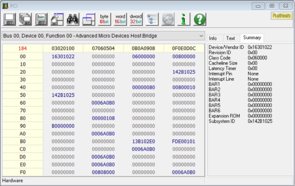
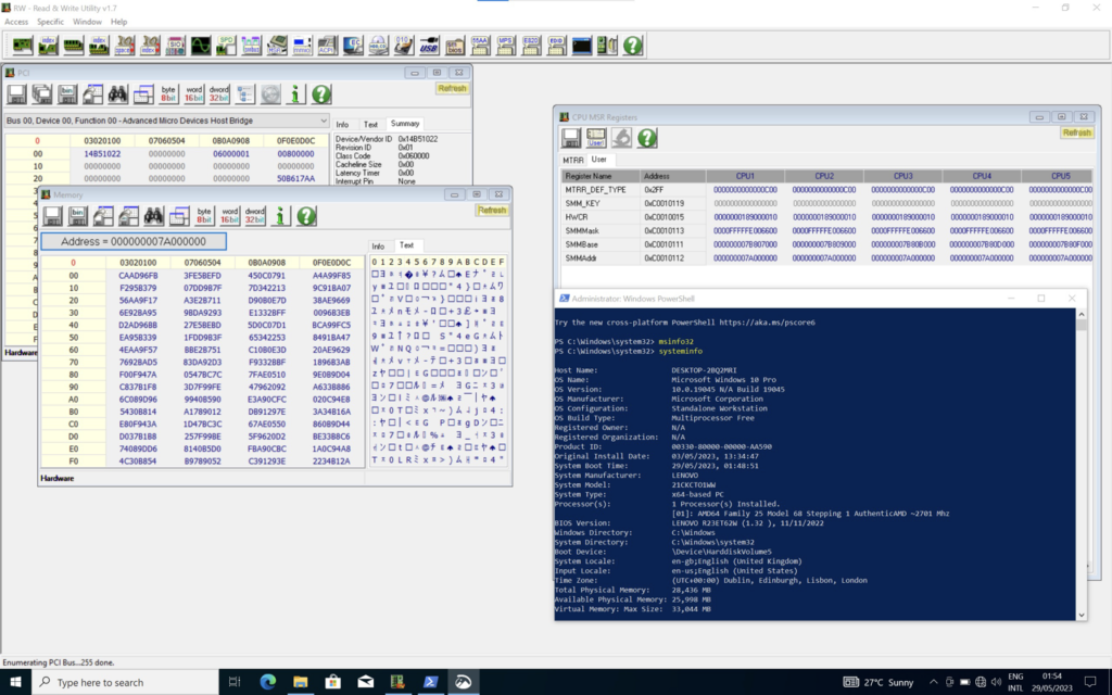
Here we found that the configuration can be checked by first determining the PSP MMIO base address and then, at a specific offset, reading out the value of two PSB-related registers.
PSP MMIO Base Address
First, the PSP MMIO base address is obtained by writing a specific value to a register of the AMD IOHUB Core (IOHC). More specifically:
0x13E102E0 for families 17h, model 30h/70h or family 19h, model 20h or
0x13B102E0 for all other models
is written to the register at offset 0xB8 of the IOHC device (on bus 00h, device 00h, function 00h) and the result is read from the register at offset 0xBC.
For example, on an Acer Swift 3 (fam 17h, model 60h) we write the value 0x13B102E0 at offset 0xB8 of the IOHC and read the base address 0xFDE00000 (after masking) at offset 0xBC.
PSB Configuration Registers
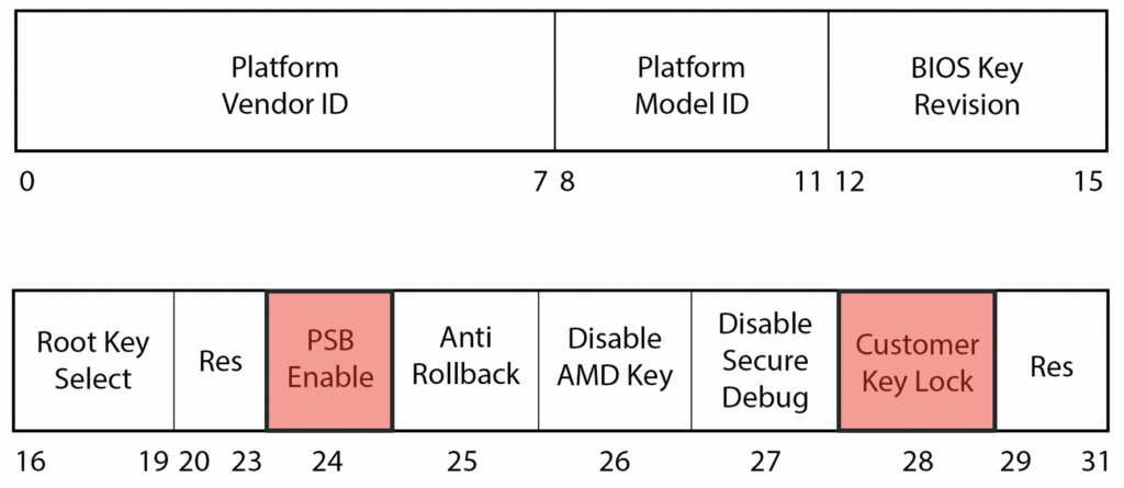
The PSB fuse register, located at offset 0x10994, reflects the actual fuse configuration and has the following structure:
It has various fields, such as:
the platform vendor ID and platform model ID to uniquely identify the platform
the BIOS key revision and anti-rollback to revoke BIOS signing keys
the AMD disable key to prevent booting a BIOS signed with the AMD root signing key
the PSB enable field to enable the feature
the customer key lock to permanently burn the fuses
We observed that on systems with the PSB enabled, typically the platform vendor ID, the platform model ID, the PSB enable bit and the customer key lock are configured accordingly. In fact, if the BIOS was compiled with the feature enabled, the fusing process occurs automatically when the system boots for the first time.
Interestingly, the PSB can also be permanently disabled by setting the PSB enable bit to 0 and the customer key lock to 1. This would enable an attacker to leave the system vulnerable indefinitely and is similar to what was discovered for Intel BootGuard by Alexander Ermolov (see Safeguarding Rootkits: Intel BootGuard at ZeroNights).
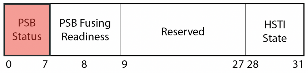
The PSB status register, located at offset 0x10998, is used for obtaining PSB state information and has the following structure:
Here we only know that the PSB status field returns 0x00 if no errors occurred; otherwise returns a non-zero value likely corresponding to a specific error code.
Vulnerabilities
Now that we understand how the PSB should be configured, we would like to walk you through misconfiguration and implementation issues we discovered during our research.
For completeness, the list of systems we tested and whether they were found to be vulnerable or not can be found in a table at the end of this blog.
Configuration flaws
Based on our knowledge of the PSB fuse and status registers, we implemented the logic into our in-house developed platform testing tool Platbox (see here) and discovered that almost none of the tested systems had the feature enabled.
As can be seen below, the Lenovo IdeaPad 1 Gen7 (BIOS JTCN44WW) did not have the PSB fuse register burned and the PSB status field returned a non-zero value. In fact, the same pattern was observed on all other vulnerable systems.
When trying to determine the root cause, we found that various data structures that are essential to the correct functioning of the PSB were missing, such as the BIOS signing key and the BIOS PEI firmware volume signature. This may indicate that already during the build process of the firmware image the feature was simply disabled.
Implementation flaws
Beyond configuration flaws, we also wanted to find out whether there were any potential implementation issues. While AMD implements the first portion of the chain-of-trust, verifying the SEC and PEI phase, we decided to focus on the vendor-specific portion that verifies the DXE phase.
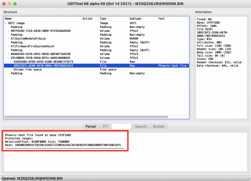
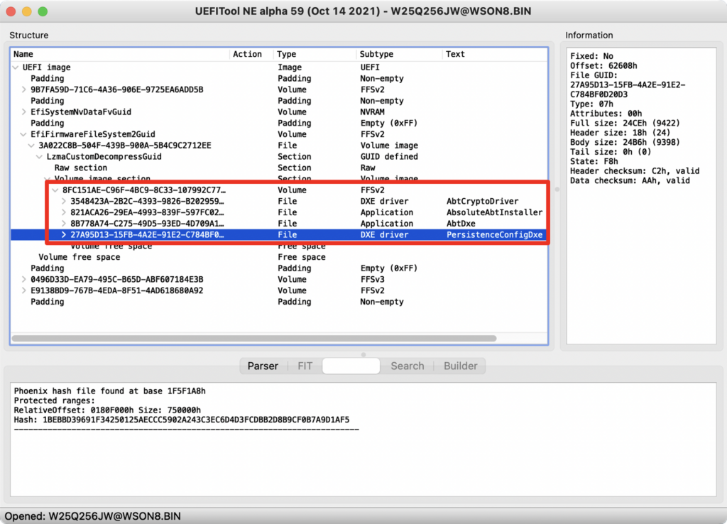
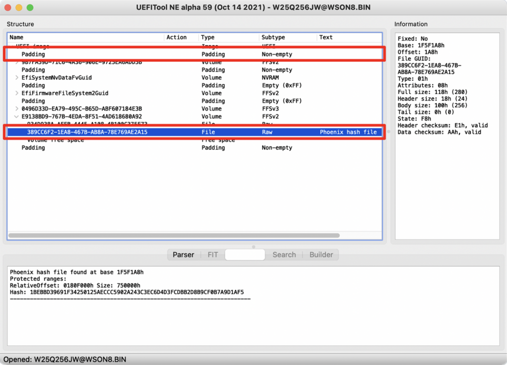
To begin, we picked the Lenovo Thinkpad P16s Gen1 (BIOS v1.32) as our target, as it was one of the few systems that had the PSB enabled, and inspected the firmware with UEFI Tool. As it turns out, it uses a Phoenix-based BIOS and a well-known data structure, called the Phoenix hash file, to verify the DXE phase:
The Phoenix hash file format is straightforward – it is a list of protected ranges of the SPI flash encoded using triples that consist of base address, size and a hash. These protected ranges should, at least in theory, cover the DXE phase code, stored in DXE firmware volumes, that will be loaded.
However, we found that that multiple firmware volumes were used and that one of them (GUID 8FC151AE-C96F-4BC9-8C33-107992C7735B) was not covered by the protected ranges. Thereby, code contained within said volume could be tampered with and it would be automatically loaded during the boot process.
To make matters worse, we noticed that while the BIOS PEI firmware volume, verified by the PSP, was located in the beginning of the firmware in the padding section, whereas the Phoenix hash file was located at the end of it and thereby could be tampered with.
To confirm that the issue was indeed exploitable, we replaced the PersistenceConfigDxe DXE driver (GUID 27A95D13-15FB-4A2E-91E2-C784BF0D20D3) with a malicious DXE driver that configures the SMM_KEY MSR and allows us, at runtime, to disable the TSEG protections and thereby trivially escalate privileges to SMM (see previous blog post for more details).
Note that an advisory was published by Lenovo (see here) for this vulnerability (assigned CVE-2023-5078) that details which systems it affected and when different BIOS updates were released.
Vendor response
As part of our responsible disclosure process, we have reached out to various vendors in order to address the issues and get an understanding of the underlying problem. The responses were, to say the least, quite surprising:
Acer
“We appreciated your information about a possible vulnerability in Acer product. After thoroughly investigation, AMD PSB is an Optional Design during develop on consumption product, it’s not a mandatory requirement in Swift 3 SF314-42;
even though AMD PSB status is not enabled by default, platform with Secure Boot and Secure Flash are in position to protect system if malicious code injecting to flash ROM, so we don’t consider this as a vulnerability.”
Lenovo
“Platform Secure Boot was introduced as a standard feature on all consumer Lenovo laptops in 2022, and laptops manufactured prior to this date were not designed with this feature in mind. Enabling it on devices now in the field would be likely to frustrate consumers if any unexpected issues arise.”
Huawei
“The PSB function was not enabled on our early AMD platform product, the PSB-like function(also known as “Intel Boot Guard”) was enabled on our later Intel platform product (such as MateBook 16s 2022).
We confirmed with the BIOS supplier (Wingtech Technology) of the AMD platform product, there is no modification plan for this issue. To avoid confusing users, we kindly ask you not to disclose this issue. […]”
Conclusions
The results of our research demonstrate how vendors systematically failed to either properly configure the platform or correctly implement the chain-of-trust. Although it is clear how this issue needs to be addressed, based on vendor responses, it appears that they are reluctant to do so.
These issues would allow an attacker that has obtained a foothold on the OS, in combination with a SPI flash write primitive (e.g. CVE-2023-28468), to install firmware implants on the system. These, by design, bypass any OS- and Hypervisor-level protections that may be implemented and, if done properly, can also be made resistant to traditional firmware updates.
To determine whether you are vulnerable, we recommend running our in-house developed tool Platbox (see here) and, if that is the case, to reach out to the vendor in the hope that they will address these issues.
Appendix
The following table lists the systems we tested and what we discovered.
INSIGHTS, RESEARCH | January 18, 2024
Owning a Bitcoin ATM
By
Antonio Requena
Gabriel Gonzalez
& Sergio Ruiz
Nowadays, Bitcoin and cryptocurrencies might look less popular than they did just a few years ago. However, it is still quite common to find Bitcoin ATMs in numerous locations.
IOActive had access to few of these machines, specifically to Lamassu’s Douro ATM (https://lamassu.is). This provided us with the opportunity to assess the security of these devices – more specifically, to attempt to achieve full control over them.
Figure 1. Lamassu Douro Bitcoin ATM
In this post, we’ll explain all the steps we followed to identify a series of vulnerabilities (CVE-2024-0175, CVE-2024-0176 and CVE-2024-0177) that allows full control over these ATMs. For this exercise, we are assuming the role of an attacker with the same physical access to the device that a regular customer might have.
Don’t Touch Me
After booting up, the screen displays the the UI for the kiosk’s primary application. However, during boot, for a few seconds the user can interact with the Linux operative system’s window manager, as illustrated in Figure 2.
Figure 2. Accessing Applications during boot
During this time, it was possible to pop up a terminal window or run any other installed application as a low-privilege user.
Look at the Camera!
In order to obtain full control over the device, the next step was to perform a privilege escalation. To achieve this, we exploited the software update mechanism by creating a file named ‘/tmp/extract/package/updatescript.js’ with the following payload:
Next, we created a file named ‘done.txt’ in the ‘/tmp/extract folder.’ This would trigger the watchdog process, which runs as root in the reviewed machines, to execute the JavaScript payload.
How did we create these files? Well, that’s an interesting question, as although we gained access to the graphical interface and the terminal, there was no keyboard plugged in. While we did have physical access to the devices, so that opening them and plugging in a keyboard would be too easy, the goal was to gain control without invasive physical access, therefore we explored a different approach.
The ATM supports a feature that enables it to read QR codes, and the binary located at ‘/usr/bin/zbarcam’ could be executed using the touch controls, so we only had to use a custom QR code containing our payload. Once the payload was read, a root shell was popped.
The following video illustrates the paths we followed to exploit the vulnerability.
Once we gained root access, we could reasonably think that the job was done. However, we looked to the ‘/etc/shadow’ file, where we were able to crack the root password in less than one minute – and the same password was valid for all of the devices.
Disclosure Timeline
IOActive followed responsible disclosure procedures which included the following:
11th July 2023 – Initial contact to report the vulnerabilities.
9th October 2023 – The vendor confirmed the issues were fixed.
25th October 2023 – The vendor asked us to delay publishing details about the vulnerabilities.
22nd November 2023 – The vendor contacted us and published an advisory mentioning the issues were fixed.
18th January 2024 – CVEs have been published by the corresponding CNA.
The following security bulletin was released by Lamassu regarding their remediation of the security issues found by IOActive:
With the connected car now commonplace in the market, automotive cybersecurity has become the vanguard of importance as it relates to road user safety. At the forefront of transportation cybersecurity research, IOActive has amassed over a decade of real-world vulnerability data illustrating the issues and potential solutions to cybersecurity threats today’s vehicles face.
This analysis is a major update and follow-up to IOActive’s paper on vehicle vulnerabilities originally published in 2016 and updated in 2018. The goal of this 2022 update is to deliver current data and discuss how the state of automotive cybersecurity has progressed over the course of 10 years, making note of overall trends and their causes. The target audience of this research is individuals seeking insights into the trends of automotive cybersecurity, and how to better address any causalities noted within this paper.
Some of the major technical findings from IOActive’s analysis:
There was a significant drop in the proportion of critical-impact vulnerabilities from 2016 to 2018. Critical-impact vulnerabilities decreased by 15%, causing the distribution of medium- and low-impact vulnerabilities to increase.
The industry saw significant growth in incorporating cybersecurity into the design of automotive systems from the start; for example, ensuring that processes that handle data run with limited privileges, which helps lower the impact of the most likely attacks in the event of a compromise.
There was an early warning observed in 2018 that the industry appears to be focusing on severity of ease-of-exploitation over actual risk.
A sharp decrease in physical attacks was reported, which was mainly due to industry attention focusing on remote-based attack vectors.
The trends observed between 2018 and 2022 are the complete opposite to what IOActive previously observed, which indicates a bounce-back effect. High-effort vulnerabilities have decreased by 6% and medium-effort have decreased by 11%, resulting in a major increase (17%) of low-hanging fruit issues.
By
Enrique Nissim
Krzysztof Okupski
& Joseph Tartaro
Introduction
During our recent talk at HardwearIO (see here, slides here) we described a variety of AMD platform misconfigurations that could lead to critical vulnerabilities, such as:
TSEG misconfigurations breaking SMRAM protections
SPI controller misconfigurations allowing SPI access from the OS
Platform Secure Boot misconfigurations breaking the hardware root-of-trust
Here we are providing a brief overview of essential registers settings and explain how our internally developed tool Platbox (see here) can be used to verify them and ultimately exploit them.
SMM Protections
In a previous blog post about AMD platform security (see here) we explained how forgetting to set a single lock can lead to a complete compromise of System Management Mode (SMM).
To recap, on modern systems SMM lives in a protected memory region called TSEG and four Model Specific Registers (MSRs) need to be configured to guarantee these protections:
0xC0010111 (SMM_BASE; base of SMM code)
0xC0010112 (SMMAddr; defines TSEG base address)
0xC0010113 (SMMMask; defines TSEG limit and TSEG enable bit)
0xC0010015[SmmLock] (HWCR; defines lock of the aforementioned MSRs)
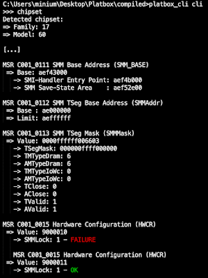
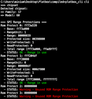
In the following we can see a breakdown of the aforementioned registers using Platbox on the Acer Swift 3 (model no. SF314-42; BIOS v1.10):
As marked in the output, the SMMLock bit in the Hardware Configuration Register (HWCR) hasn’t been set and therefore the TSEG region protections can simply be disabled by a privileged OS attacker by disabling the TValid bit in the SMMMask MSR.
Additionally, to ensure that the SMM code lies within the protected TSEG region, one should also confirm that the SMM base address (stored in the SMM_BASE MSR) lies inside of TSEG. In most cases the EDK2 framework will ensure that this is the case. It is also interesting to notice that SMM_BASE is also locked when SMMLock is set, thus preventing relocation attacks.
One additional register that is relevant to the security of SMM is the SMM key register (stored in the SMM_KEY MSR at 0xC0010119; see p630 in [1]). This is a write-only MSR that can be set before SMMLock to create a password-protected mechanism to clear SMMLock later on.
As mentioned in our presentation, while we haven’t found an OEM using this register, we used it as part of an exploit to demonstrate persistence in vulnerable platforms.
SPI Flash Protections
The SPI flash plays an important role in the context of platform security as it is used to store both the UEFI BIOS firmware code and configuration data (e.g. the Secure Boot state).
Architecturally, firmware code should only be modified at boot-time during firmware updates (via signed capsule updates) whereas portions of configuration data can be modified at run-time (in a controlled way via SMM).
To enforce this, the SPI controller-related protections need to be configured accordingly. In the following we will explain the relevant protection mechanisms, both the classic ones and the modern ones that will soon replace them.
Classic Protections
Two classic protection mechanisms exist, referred to as ROM protected ranges and SPI restricted commands, each responsible for preventing different types of accesses (see p445 in [2]).
First, ROM protected ranges apply to direct accesses via memory-mapped IO which, in turn, are automatically translated by the hardware into transactions on the SPI bus.
These ranges are configured via four write-once ROM protect registers (see p440 in [2]):
D14F3x050 FCH::ITF::LPC::RomProtect0
D14F3x054 FCH::ITF::LPC::RomProtect1
D14F3x058 FCH::ITF::LPC::RomProtect2
D14F3x05C FCH::ITF::LPC::RomProtect3
As we can see below, each of these registers defines the base address, the size and the access protection (read / write):
At the same time, it is important to enable and lock the ROM protected ranges with the AltSPICS register (see p450 in [2]):
SPIx01D FCH::ITF::SPI::AltSPICS[SpiProtectEn0]
SPIx01D FCH::ITF::SPI::AltSPICS[SpiProtectEn1]
SPIx01D FCH::ITF::SPI::AltSPICS[SpiProtectLock]
However, we observed that although some systems don’t configure these ranges, we haven’t been able to perform writes to the SPI flash using this method neither from the OS nor from SMM.
Second, SPI restricted commands apply to indirect accesses via the SPI controller wherein SPI registers are programmed directly. As part of it, two restricted command registers are configured (see p447-448 in [2]):
SPIx004 FCH::ITF::SPI::SPIRestrictedCmd
SPIx008 FCH::ITF::SPI::SPIRestrictedCmd2
Each of these registers defines up to four SPI opcodes that are blocked. Again, we can see the breakdown below:
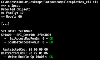
In this example we can see that SPI writes are blocked altogether by restricting the Write Enable (WREN) opcode that needs to be sent before every SPI write operation.
In practice, when SMM code needs to perform a SPI write transaction it will temporarily disable the restricted command registers, perform the write operation and then restore the restricted command registers again.
In case these protections are misconfigured, as we have observed on various systems, a privileged OS attacker can easily exploit this issue. In the following we see a simple proof-of-concept that will patch portions of the SPI flash (see here):
In short, the code will first print the portion of the flash that is to be patched. It will then patch it, and finally print the modified flash portion again. The amd_spi_write_buffer() API automatically handles reading the affected SPI flash pages, patching them and writing them back.
Modern SPI Protections
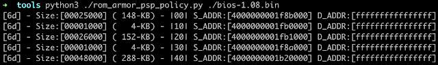
On more modern systems we have observed that the aforementioned protection mechanisms are slowly being replaced by a newer technology referred to as ROM Armor.
In essence, ROM Armor is AMD’s equivalent of Intel’s Protected Range Registers (PRRs) and ensures that only whitelisted portions of the SPI flash can be modified at run-time (in a controlled fashion via SMM).
To determine which portions of the SPI flash are whitelisted, we developed a script that parses the PSP directory and extracts the whitelisted regions (see here):
Note that in this case we used an Acer TravelMate P4 (model no. TMP414-41-R854; BIOS v1.08) instead as this technology is only present in most recent systems.
Hardware Root-of-Trust Configurations
Platform Secure Boot (PSB) is AMD’s implementation of a hardware root-of-trust and ensures that initial phases of the UEFI BIOS firmware haven’t been tampered with and is the main line of defense against persistent firmware implants.
PSB is implemented using an embedded chip called the Platform Security Processor (PSP). In order for PSB to be enforced, the UEFI BIOS firmware needs to be built accordingly and the PSB related fuses in the PSP need to be configured.
We’ve found that two registers in particular can be leveraged to determine whether PSB has been enabled correctly:
PSB Fuse Register (defines fuse configuration)
PSB State Register (defines configuration state)
While the PSB fuse register can be used to determine whether PSB has been enabled and the fuses have been locked, the PSB state register indicates the status of the PSB configuration.
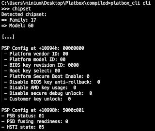
Herein we can see a more detailed breakdown of these registers:
As we can see, the Acer Swift 3 does not properly configure the PSB fuses and the PSB status indicates that an error has occurred.
The following video demonstrates how the ability to write to the SPI flash (via an SMI vulnerability or SPI controller misconfigurations), combined with the lack of PSB, results in a persistent firmware implant.
First, we attempt to read the TSEG region and see that it’s not accessible as it returns FFs only. We therefore patch the firmware with our backdoor inside of it via a vulnerable SMI handler and reset the system:
Next, we attempt to read the TSEG region again and see that the result is the same. However, this time around after disabling the TSEG protections via the SMM_KEY that was configured by our backdoor, we are able to read it out:
Here is the proof-of-concept that leverages the SMM key configured by the backdoor, clears the SmmLock bit in the HWCR register and finally disables TSEG protections (see here):
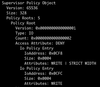
The SMM Supervisor is AMD’s approach at deprivileging and isolating SMI handlers. When implemented, SMI handlers need to go through an enforcement module to gain access to MSRs and IO registers. Additionally, paging is added which limits their access to arbitrary system memory. Everytime an SMI attempts to access these privileged resources, an OEM policy is checked to see if they can have access or not.
OEM policies live within the Freeform Blob called SmmSupvBin with the GUID {83E1F409-21A3-491D-A415B163A153776D}. The policy contains multiple types of entries:
Memory
IO Register
MSR
Instruction
SaveState
A small utility is available in the Platbox repository (see here). This utility will attempt to parse UEFI images and extract the policy, or if you provide a raw policy format that has been previously extracted it will print the details.
For example, this is a section of an OEM policy which is specifically restricting IO Register Write access to the IO Registers 0xCF8 and 0xCFC, thus specifically restricting access to PCI configuration space. We believe that this will come in handy in the future to perform baseline comparisons against OEM policies across various platforms. It gives researchers the ability to quickly see if an OEM failed to restrict a specific MSR or IO Register which may aid an attacker.
Resources
[1] AMD64 Architecture Programmer’s Manual, Volume 2: System Programming [2] Processor Programming Reference (PPR) for AMD Family 17h Model 20h, Revision A1 Processors
INSIGHTS, RESEARCH | June 13, 2023
Applying Fault Injection to the Firmware Update Process of a Drone
By
Gabriel Gonzalez
IOActive recently published a whitepaper covering the current security posture of the drone industry. IOActive has been researching the possibility of using non-invasive techniques, such as electromagnetic (EM) side-channel attacks or EM fault injection (EMFI), to achieve code execution on a commercially available drone with significant security features. For this work, we chose one of the most popular drone models, DJI’s Mavic Pro. DJI is a seasoned manufacturer that emphasizes security in their products with features such as signed and encrypted firmware, Trusted Execution Environment (TEE), and Secure Boot.
Attack Surface
Drones are used in variety of applications, including military, commercial, and recreational. Like any other technology, drones are vulnerable to various types of attacks that can compromise their functionality and safety.
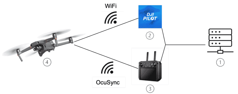
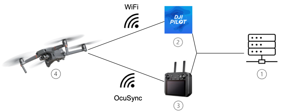
As illustrated above, drones expose several attack surfaces: (1) backend, (2) mobile apps, (3) radio frequency (RF) communication, and (4) physical device.
As detailed in the whitepaper, IOActive used EM emanations and EMFI due to their non-invasive nature. We leveraged Riscure products as the main tools for this research.
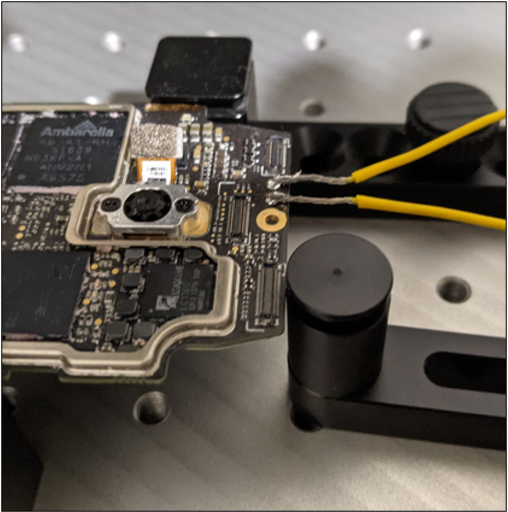
The image below show the PCB under analysis after being removed from the drone; power has been connected to an external power supply.
First Approach
Our first approach was to attempt to retrieve the encryption key using EM emanations and decrypting the firmware. We started by finding an area on the drone’s PCB with a strong EM signal so we could place a probe and record enough traces to extract the key.
After identifying the location with strongest signal, we worked on understanding how to bypass the signature verification that takes place before the firmware is decrypted. After several days of testing and data analysis, we found that the probability of successful signature bypass was less than 0.5%. This rendered key recovery unfeasible, since it would have required us to collect the tens of thousands of traces.
Second Approach
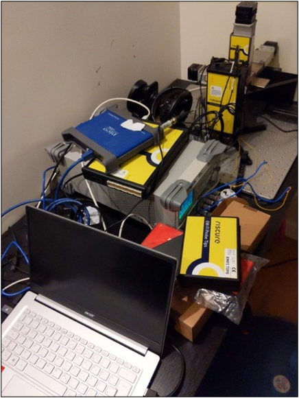
Our second approach was to use EMFI based on the ideas published by Riscure (https://www.riscure.com/publication/controlling-pc-arm-using-fault-injection). Riscure proposes using a glitch to cause one instruction to transform into another and gain control of, for example, the PC register. The following image shows the setup we used for this approach, which included a laptop (used as a controller), a power supply, Riscure’s Spider (used to generate the trigger), an oscilloscope, an XYZ table, and the EMFI pulse-generator.
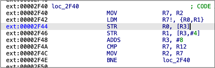
After identifying a small enough area on the PCB, we modified the glitch’s shape and timing until we observed a successful result. The targeted process crashed, as shown below:
Our payload appeared in several registers. After examining the code at the target address, we determined that we had hit a winning combination of timing, position, and glitch shape. The following capture shows the instruction where a segmentation error took place:
The capture clearly shows a load instruction copying our data to registers R0 and R1. In addition, the GDB output also shows that registers R3 and R4 ended up with controlled data. Further details can be found in the whitepaper.
Having successfully caused memory corruption, the next step would be to design a proper payload that achieves code execution. An attacker could use such an exploit to fully control one device, leak all sensitive content, enable ADB access, and potentially leak the encryption keys.
Disclosure Timeline
The DJI team response was excellent, fast and supportive.
2023-04-04: Initial Contact with DJI including sharing report. 2023-05-04: DJI agrees on publication date.
RESEARCH |
Drone Security and Fault Injection Attacks | Gabriel Gonzalez | IOActive Labs Blog
By
Gabriel Gonzalez
I recently published the full technical details to the research in this IOActive whitepaper.
The use of Unmanned Aerial Vehicles (UAVs), commonly referred to as drones, continues to grow. Drones implement varying levels of security, with more advanced modules being resistant to typical embedded device attacks. IOActive’s interest is in developing one or more viable Fault Injection attacks against hardened UAVs.
IOActive has been researching the possibility of achieving code execution on a commercially available drone with significant security features using non-invasive techniques, such as electromagnetic (EM) side-channel attacks or EM fault injection (EMFI). For this work, we chose one of the most common drone models, DJI’s Mavic Pro. DJI is a well established manufacturer that emphasizes security in their products, such as signed and encrypted firmware, Trusted Execution Environment (TEE), and Secure Boot.
Adventures in the Platform Security Coordinated Disclosure Circus
By
Enrique Nissim
Krzysztof Okupski
& Joseph Tartaro
Platform security is one of the specialized service lines IOActive offers and we have worked with many vendors across the industry. Lately, we have been conducting research on various targets while developing tooling that we believe will help the industry make platform security improvements focused on AMD systems.
SecSMIFlash
In early October 2022, IOActive reported a number of security issues to ASUS and AMI in an SMM module called SecSMIFlash (GUID 3370A4BD-8C23-4565-A2A2-065FEEDE6080). SecSMIFlash is included in BIOS image G513QR.329 for the ASUS Rog Strix G513QR. This module garnered some attention after Alexander Matrosov (BlackHat USA 2017) demonstrated how the SMI handlers failed to check input pointers with SmmIsBufferOutsideSmmValid(), resulting in CVE-2017-11315.
IOActive discovered issues on one of our target platforms, a fully updated ASUS Rog Strix G513QR, while running an internally developed dumb SW SMI fuzzer. Almost immediately, the system appeared to hang on SMI handler 0x1D.
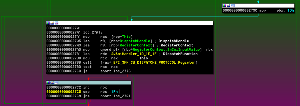
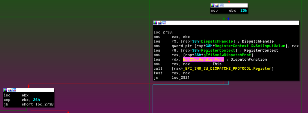
This module registers a single SW SMI handler for three different SwSmiInputs (0x1D, 0x1E, 0x1F) via EFI_SMM_SW_DISPATCH2_PROTOCOL:
Based on public information about this module, the above operations map to:
– 0x1D – LOAD_IMAGE
– 0x1E – GET_POLICY
– 0x1F – SET_POLICY
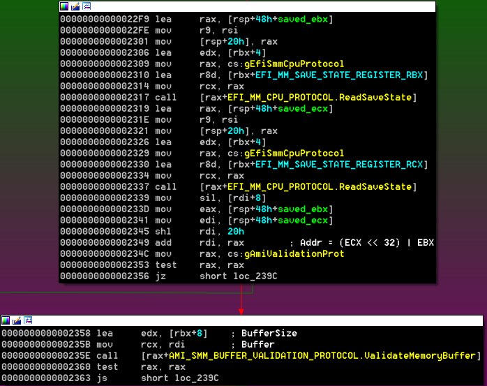
The handler uses EFI_MM_CPU_PROTOCOL to read the contents of the saved ECX and EBX registers and create a 64-bit pointer. This constructed buffer is verified to be exactly 8 bytes long and outside SMRAM using AMI_SMM_BUFFER_VALIDATION_PROTOCOL:
Depending on the value written on the SW-SMI triggering port (SwSmiInput), the execution continues in handle_load_image (0x1D), handle_get_policy (0x1E), or handle_set_policy (0x1F). These three functions receive a single argument which is the constructed pointer from the previous step:
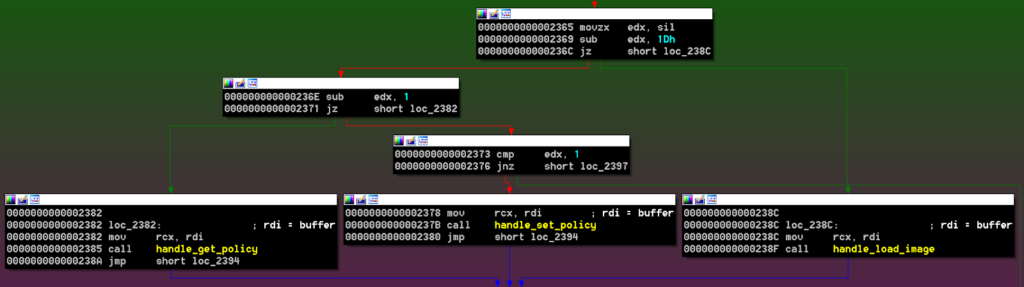
The three operations have security issues.
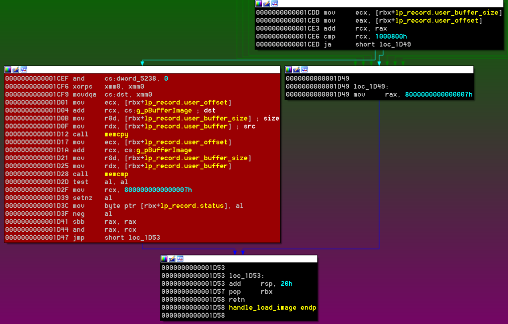
Let’s start with handle_load_image. As part of its initialization, SecSMIFlash allocates 0x1001 pages of memory (g_pBufferImage) that are going to be used to store the BIOS image file.
The buffer address is put into RBX and then validated again but this time it checks that the size is at least 0x18 bytes (outside SMRAM).
The buffer is used as a record defined as follows:
typedef struct { /* 0x00 */ void * user_buffer; /* 0x08 */ unsigned int user_offset; /* 0x0C */ unsigned int user_buffer_size; /* 0x10 */ unsigned int status; /* 0x14 */ unsigned int unk; } lp_record;
Another pointer is extracted from memory (the user_buffer member), which is validated to be user_buffer_size bytes, followed by a check that attempts to make sure that the provided offset and size are within the allocated bounds of g_pBufferImage.
The problem is that there is a time-of-check to time-of-use (TOCTOU) condition that can be abused:
The block of code that performs the checks does not make local copies of the values into SMRAM. The values are retrieved again from user-controlled memory when the copy is done, which means the values could have changed.
Exploitation of this issue requires the use of a DMA agent.
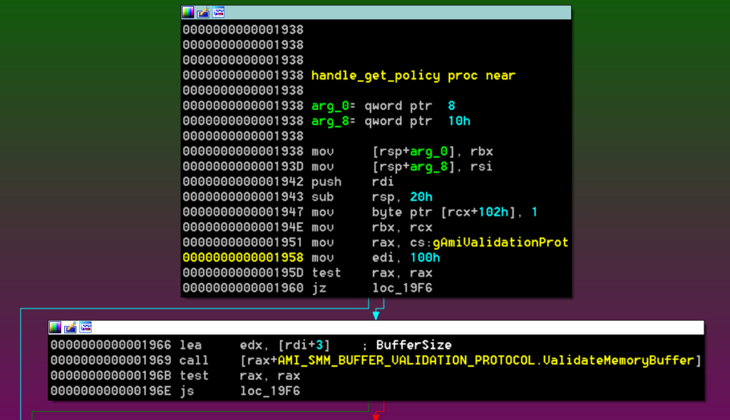
In the case of the handle_get_policy operation, the code presents a vulnerability in the first basic block:
Previously, the buffer was verified to only 8 bytes outside SMRAM, but here the code writes the value 1 at offset +102h and the ValidateMemoryBuffer check happens afterwards. Moreover, if ValidateMemoryBuffer fails, the handler simply bails out without doing anything else.
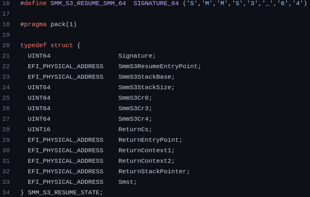
This out-of-bounds write condition allows the first 250 bytes (102h – 8) of the TSEG region to be written. The bottom of the TSEG region contains the SMM_S3_RESUME_STATE structure:
There are several EFI_PHYSICAL_ADDRESS pointers that could be targeted to achieve arbitrary SMM code execution.
The following PoC code uses Platbox and the above primitive to write ones to the first 250 bytes of the TSEG region (0xef000000 in the machine used for testing):
Finally, for the handle_set_policy operation, the code suffers from a combination of the issues described above.
Responsible Disclosure Attempt
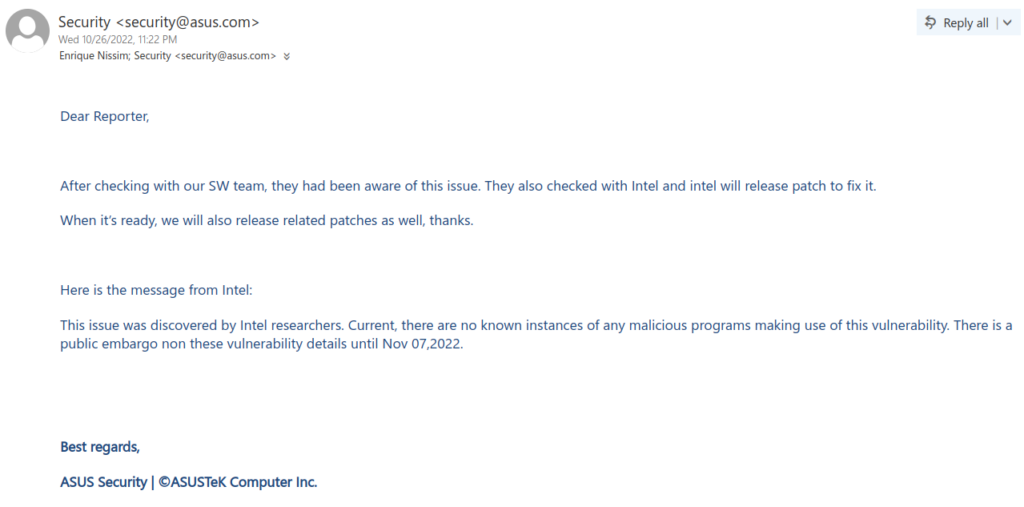
IOActive drafted a technical document and sent it over to ASUS. After a few weeks, ASUS replied with the following:
The response left us with some concerns:
1. They claimed all the reported issues were known by the team. 2. There was no ETA for the patch. 3. The issues were discovered by Intel and there was an embargo? 4. Is there a CVE assigned to track these?
We replied with a few questions along these lines and their response made it clear that the module is entirely handled by AMI and that Intel researchers may or may not apply a CVE number.
On the other hand, AMI provided a much quicker response, although quite unexpected:
Thursday, February 16, 2023
Adventures in the Platform Security Coordinated Disclosure Circus
Platform security is one of the specialized service lines IOActive offers and we have worked with many vendors across the industry. Lately, we have been conducting research on various targets while developing tooling that we believe will help the industry make platform security improvements focused on AMD systems.
SecSMIFlash
In early October 2022, IOActive reported a number of security issues to ASUS and AMI in an SMM module called SecSMIFlash (GUID 3370A4BD-8C23-4565-A2A2-065FEEDE6080). SecSMIFlash is included in BIOS image G513QR.329 for the ASUS Rog Strix G513QR. This module garnered some attention after Alexander Matrosov (BlackHat USA 2017) demonstrated how the SMI handlers failed to check input pointers with SmmIsBufferOutsideSmmValid(), resulting in CVE-2017-11315.
IOActive discovered issues on one of our target platforms, a fully updated ASUS Rog Strix G513QR, while running an internally developed dumb SW SMI fuzzer. Almost immediately, the system appeared to hang on SMI handler 0x1D.
This module registers a single SW SMI handler for three different SwSmiInputs (0x1D, 0x1E, 0x1F) via EFI_SMM_SW_DISPATCH2_PROTOCOL:
Based on public information about this module, the above operations map to:
– 0x1D – LOAD_IMAGE
– 0x1E – GET_POLICY
– 0x1F – SET_POLICY
The handler uses EFI_MM_CPU_PROTOCOL to read the contents of the saved ECX and EBX registers and create a 64-bit pointer. This constructed buffer is verified to be exactly 8 bytes long and outside SMRAM using AMI_SMM_BUFFER_VALIDATION_PROTOCOL:
Depending on the value written on the SW-SMI triggering port (SwSmiInput), the execution continues in handle_load_image (0x1D), handle_get_policy (0x1E), or handle_set_policy (0x1F). These three functions receive a single argument which is the constructed pointer from the previous step:
The three operations have security issues.
Let’s start with handle_load_image. As part of its initialization, SecSMIFlash allocates 0x1001 pages of memory (g_pBufferImage) that are going to be used to store the BIOS image file.
The buffer address is put into RBX and then validated again but this time it checks that the size is at least 0x18 bytes (outside SMRAM).
The buffer is used as a record defined as follows:
typedef struct { /* 0x00 */ void * user_buffer; /* 0x08 */ unsigned int user_offset; /* 0x0C */ unsigned int user_buffer_size; /* 0x10 */ unsigned int status; /* 0x14 */ unsigned int unk;} lp_record;
Another pointer is extracted from memory (the user_buffer member), which is validated to be user_buffer_size bytes, followed by a check that attempts to make sure that the provided offset and size are within the allocated bounds of g_pBufferImage.
The problem is that there is a time-of-check to time-of-use (TOCTOU) condition that can be abused:
The block of code that performs the checks does not make local copies of the values into SMRAM. The values are retrieved again from user-controlled memory when the copy is done, which means the values could have changed.
Exploitation of this issue requires the use of a DMA agent.
In the case of the handle_get_policy operation, the code presents a vulnerability in the first basic block:
Previously, the buffer was verified to only 8 bytes outside SMRAM, but here the code writes the value 1 at offset +102h and the ValidateMemoryBuffer check happens afterwards. Moreover, if ValidateMemoryBuffer fails, the handler simply bails out without doing anything else.
This out-of-bounds write condition allows the first 250 bytes (102h – 8) of the TSEG region to be written. The bottom of the TSEG region contains the SMM_S3_RESUME_STATE structure:
There are several EFI_PHYSICAL_ADDRESS pointers that could be targeted to achieve arbitrary SMM code execution.
The following PoC code uses Platbox and the above primitive to write ones to the first 250 bytes of the TSEG region (0xef000000 in the machine used for testing):
Finally, for the handle_set_policy operation, the code suffers from a combination of the issues described above.
Responsible Disclosure Attempt
IOActive drafted a technical document and sent it over to ASUS. After a few weeks, ASUS replied with the following:
The response left us with some concerns:
1. They claimed all the reported issues were known by the team.
2. There was no ETA for the patch.
3. The issues were discovered by Intel and there was an embargo?
4. Is there a CVE assigned to track these?
We replied with a few questions along these lines and their response made it clear that the module is entirely handled by AMI and that Intel researchers may or may not apply a CVE number.
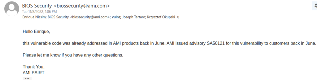
On the other hand, AMI provided a much quicker response, although quite unexpected:
We attempted to look for advisory SA50121 but did not find anything. It is probably only available to vendors. What is surprising though, is they say that a fix was released in June.
SMIFlash
At this point, we decided to look at the other related module Alex Matrosov’s presentation: SMIFlash.efi. SMIFlash (GUID BC327DBD-B982-4F55-9F79-056AD7E987C5) is one of the SMM modules included in BIOS image G513QR.330 for the ASUS Rog Strix G513QR. The module installs six SW-SMI handlers that are prone to double fetches (TOCTOU) that, if successfully exploited, could be leveraged to execute arbitrary code in System Management Mode (ring-2).
There are two public CVEs related to this module from 2017:
CVE-2017-3753 states that the module lacks proper input pointer sanitization and only mentions Lenovo as affected; however, this module is also part of our target ASUS Rog Strix BIOS, and after a bit of reverse engineering, we were able to identify three race conditions (TOCTOU) with different levels of impact.
This module registers a single SW-SMI handler for six different SwSmiInputs (0x20, 0x21, 0x22, 0x23, 0x24, and 0x25) via EFI_SMM_SW_DISPATCH2_PROTOCOL:
Based on public information about this module, the above operations map to:
The handler uses EFI_MM_CPU_PROTOCOL to read the content of the saved ECX and EBX registers and create a 64-bit pointer. For all operations except for GET_INFO, this constructed address is verified to be exactly 18h bytes outside SMRAM using AMI_SMM_BUFFER_VALIDATION_PROTOCOL. 18h is therefore the size of the basic input record this module needs to work with. Reverse engineering the structure led to the following layout:
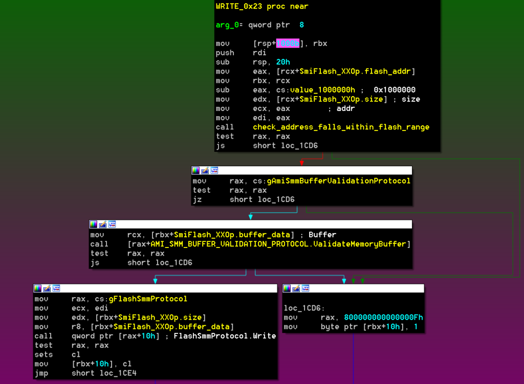
Depending on the value written on the SW-SMI triggering port (SwSmiInput), the execution continues in one of the previously listed operations (ENABLE, READ, WRITE, etc.).
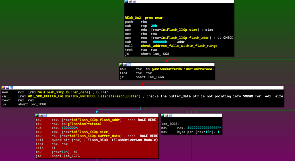
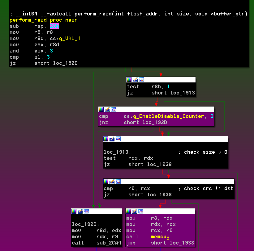
The READ and WRITE operations receive the pointer to the record as an argument and both are prone to the same TOCTOU vulnerabilities. Let’s look at the READ implementation:
RCX holds the controlled pointer and is copied into RBX. The function starts by checking that the flash_addr value falls within the intended flash range MMIO (0xFF000000-0xFFFFFFFF). It continues by using AMI_SMM_BUFFER_VALIDATION_PROTOCOL to ensure that the buffer_data pointer resides outside SMRAM. This is interesting because the reported issues in CVE-2017-3753 and CVE-2017-11316 seem to be related to the lack of validation over the input parameters. If the input pointers are not properly verified using SmmIsBufferOutsideSmmValid() (in this case ValidateMemoryBuffer()), an attacker can pass a pointer with an SMRAM address value and have the ability to read and/or write to SMRAM. In our current version, this is not the case and we can see verification is there.
Nevertheless, the code is retrieving the values from memory twice for all three members (flash_addr, size, and buffer_data). This means that the checked values do not necessarily correspond to the ones being passed to the FlashDriverSmm module. This is a race condition that an attacker can exploit through a DMA attack. Such an attack can easily be performed with a custom PCI device (e.g. PciLeech – https://github.com/ufrisk/pcileech).
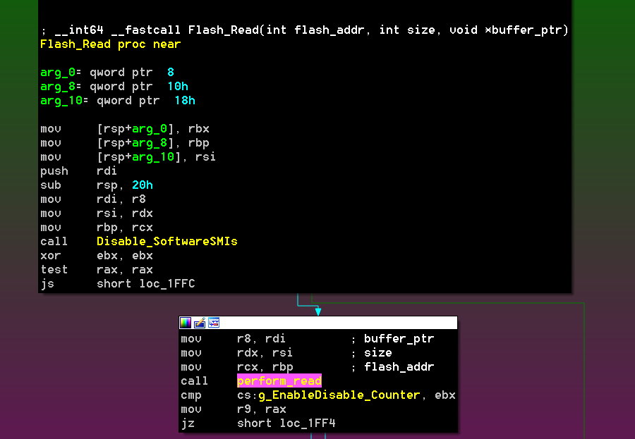
Winning the race for the READ operation leads to writing to SMRAM with values retrieved from flash; however, by disabling the Flash with the DISABLE operation first, the underlying implementation of FLASH_SMM_PROTOCOL (which resides in the FlashDriverSmm module), will use a simple memcpy to fulfill the request:
This is interesting because it provides an easier way to control all the bytes being copied.
The WRITE operation has the exact same condition, although in this case, winning the race means leaking content from SMRAM into the Flash:
In summary, for both cases, the block of code performing the checks does not make local copies of the values into SMRAM. The values are retrieved again from user-controlled memory when they are about to be used, which means the values could have changed.
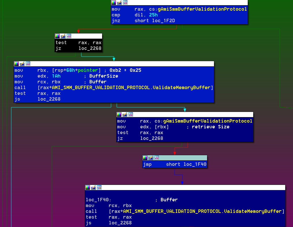
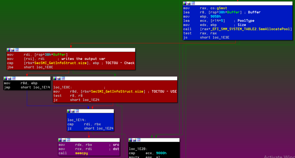
The GET_INFO (0x25) operation is affected by the same condition, although in a different way. In this case, as soon as the user pointer is constructed, the code verifies it is at least 1Ah bytes outside of SMRAM. Then, it retrieves the value of the first dword and uses it to further check the length of the provided region:
The reversed engineered structure looks as follows:
The code continues by calling into a function that allocates 905Bh bytes of SMRAM and attempts to copy the data into it. RBX is the pointer to the record, and the double-fetch is clear:
The code is trying to enforce 905Bh bytes as an upper limit for the copy but because the memory is fetched twice, the value could have changed after the check passed. As a result, SMRAM will be corrupted.
Responsible Disclosure Attempt
Q4 is always busy, and as a consequence, our team did not immediately report these issues to ASUS or AMI. Instead, four months passed since our initial report on SecSMIFlash.efi. On February 2 2023, after verifying the issues were still present in the latest available BIOS for our target ASUS laptop, we documented the findings and reported them to AMI.
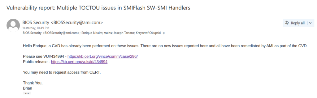
This time AMI’s response only took two hours:
The CERT link was very helpful because it allowed us to better understand the full picture. The most important sections of the vulnerability note are reproduced below:
Multiple race conditions due to TOCTOU flaws in various UEFI Implementations
Vulnerability Note VU#434994
Original Release Date: 2022-11-08 | Last Revised: 2023-01-25
Overview Multiple Unified Extensible Firmware Interface (UEFI) implementations are vulnerable to code execution in System Management Mode (SMM) by an attacker who gains administrative privileges on the local machine. An attacker can corrupt the memory using Direct Memory Access (DMA) timing attacks that can lead to code execution. These threats are collectively referred to as RingHopper attacks.
Description The UEFI standard provides an open specification that defines a software interface between an operating system (OS) and the device hardware on the system. UEFI can interface directly with hardware below the OS using SMM, a high-privilege CPU mode. SMM operations are closely managed by the CPU using a dedicated portion of memory called the SMRAM. The SMM can only be entered through System Management Interrupt (SMI) Handlers using a communication buffer. SMI Handlers are essentially a system-call to access the CPU’s SMRAM from its current operating mode, typically Protected Mode.
A race condition involving the access and validation of the SMRAM can be achieved using DMA timing attacks that rely on time-of-use (TOCTOU) conditions. An attacker can use well-timed probing to try and overwrite the contents of SMRAM with arbitrary data, leading to attacker code being executed with the same elevated-privileges available to the CPU (i.e., Ring -2 mode). The asynchronous nature of SMRAM access via DMA controllers enables the attacker to perform such unauthorized access and bypass the verifications normally provided by the SMI Handler API.
The Intel-VT and Intel VT-d technologies provide some protection against DMA attacks using Input-Output Memory Management Unit (IOMMU) to address DMA threats. Although IOMMU can protect from DMA hardware attacks, SMI Handlers vulnerable to RingHopper may still be abused. SMRAM verification involving validation of nested pointers adds even more complexity when analyzing how various SMI Handlers are used in UEFI.
Impact An attacker with either local or remote administrative privileges can exploit DMA timing attacks to elevate privileges beyond the operating system and execute arbitrary code in SMM mode (Ring -2). These attacks can be invoked from the OS using vulnerable SMI Handlers. In some cases, the vulnerabilities can be triggered in the UEFI early boot phases (as well as sleep and recovery) before the operating system is fully initialized.
[..]
Acknowledgements Thanks to the Intel iStare researchers Jonathan Lusky and Benny Zeltser who discovered and reported this vulnerability.
It is notable that there is no mention of SecSMIFlash.efi or SMIFlash.efi, and the information provided is quite generic. Nevertheless, we can see that the original release date matches what ASUS first said. It is also interesting that the vulnerability was last updated only a few days ago (Dell latest update). Additionally, the description refers to “RingHopper attacks” and mentions the Intel researchers that reported the issues.
These pieces of information immediately led to the following tweet:
Although we cannot be certain that they reported the exact same issues that we attempted to report, it does seem these two researchers documented findings on these modules before our team. It appears that the vulnerabilities were assigned CVE-2021-33164.
On November 16, 2022, Benny Zeltser tweeted that they had to withdraw the presentation from BlackHat USA and DefCon because the issues were not yet fixed. This suggests that a lot of the affected vendors have not been able to produce a new BIOS image, including the fixed modules. Indeed, from the list of vendors shown in the CERT vulnerability note, only AMI, Dell, HPE, Insyde, and Intel are marked as “affected.” We can now confirm that ASUSTeK is also affected.
Conclusion
Responsible coordinated disclosure in the platform security space is a bit of a circus. This issue was highlighted by Matrosov himself in his 2022 presentation at OffensiveCon.
ASUS mentioned an embargo that, to the best of our knowledge, expired on November 2, 2022. When reading the CERT link from AMI, all reported vendors reference CVE-2021-33164, specifically calling out issues on Intel NUCs and mentioning that the patches were released back in June of 2022. When analyzing the affected vendors list on the CERT page, you will find that all vendors noted as affected have released patches as of February 3, 2023. All vendors listed as unknown, or in our case ASUS, have yet to release patches but have been well aware of the vulnerabilities and the reports based on the communication we had with them.
IOActive has decided to publish the technical details about these issues after understanding that AMI released patches back in mid-2022 and that no new information was provided by us in our report of both modules. In addition, the CVE was filed back in 2021 and all vendors appear to have had more than enough time to responsibly patch and disclose these issues to consumers.
The CERT advisory refers to these threats as RingHopper attacks. The abstract of a presentation about RingHopper suggests billions of devices are affected by these issues. Our efforts to report these vulnerabilities to vendors stopped with the replies that they were already aware of these issues and have remedies in place. The fact that some vendors appear to still be vulnerable at this time is surprising. Ultimately, we feel it’s more important to shed light on this in order to get the issues fixed on those platforms that appear to be delayed, instead of leaving consumers and the industry in the dark for such an extended period of time.