INSIGHTS | January 24, 2008

ATMEGA88 Teardown

An 8k FLASH, 512 bytes EEPROM, 512 bytes SRAM CPU operating 1:1 with the external world unlike those Microchip PIC’s we love to write up about :).

It’s a 350 nanometer (nm), 3 metal layer device fabricated in a CMOS process.  It’s beautiful to say the least;  We’ve torn it down and thought we’d blog about it!

The process Atmel uses on their .35 micrometer (um) technology is awesome.

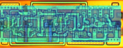
Using a little HydroFluoric Acid (HF) and we partially removed the top metal layer (M3).  Everything is now clearly visible for our analysis. After delaying earlier above, we can now recognize features that were otherwise hidden such as the Static RAM (SRAM) and the 32 working registers.

As we mentioned earlier, we used the word, “awesome” because check this out- It’s so beautifully layed out that we can etch off just enough of the top metal layer to leave it’s residue so it’s still visible depending on the focal point of the microscope!  This is very important.

We removed obscuring metal but can still see where it went (woot!).The two photos above contain two of the 30+ configuration fuses present however it makes a person wonder why did Atmel cover the floating gate of the upper fuse with a plate of metal (remember the microchip article with the plates over the floating gates?)

We highlighted a track per fuse in the above photos.  What do you think these red tracks might represent?

INSIGHTS | January 22, 2008

Security Mechanism of PIC16C558,620,621,622

Last month we talked about the structure of an AND-gate layed out in Silicon CMOS.  Now, we present to you how this AND gate has been used in Microchip PICs such as PIC16C558, PIC16C620, PIC16C621, PIC16C622, and a variety of others.

If you wish to determine if this article relates to a particular PIC you may be in possession of, you can take an windowed OTP part (/JW) and set the lock-bits.  If after 10 minutes in UV, it still says it’s locked, this article applies to your PIC.

IF THE PART REMAINS LOCKED, IT CANNOT BE UNLOCKED SO TEST AT YOUR OWN RISK.

The picture above is the die of the PIC16C558 magnified 100x.  The PIC16C620-622 look pretty much the same.  If there are letters after the final number, the die will be most likely, “shrunk” (e.g. PIC16C622 vs PIC16C622A).

Our area of concern is highlighted above along with a zoom of the area.

When magnified 500x, things become clear.  Notice the top metal (M2) is covering our DUAL 2-Input AND gate in the red box above.We previously showed you one half of the above area.  Now you can see that there is a pair of 2-input AND gates.  This was done to offer two security lock-bits for memory regions (read the datasheet on special features of the CPU).Stripping off that top metal (M2) now clearly shows us the bussing from two different areas to keep the part secure.  Microchip went the extra step of covering the floating gate of the main easilly discoverable fuses with metal to prevent UV from erasing a locked state.  The outputs of those two fuses also feed into logic on the left side of the picture to tell you that the part is locked during a device readback of the configuration fuses.

This type of fuse is protected by multiple set fuses of which only some are UV-erasable.

The AND gates are ensuring all fuses are erased to a ‘1’ to “unlock” the device.

What does this mean to an attacker?  It means, go after the inal AND gate if you want to forcefully unlock the CPU.  The outputs of the final AND gate stage run underneather VDD!! (The big mistake Microchip made).  Two shots witha laser-cutter and we can short the output stages “Y” from the AND-gate to a logic ‘1’ allowing readback of the memories (the part will still say it is locked).Stripping off the lower metal layer (M1) reveils the Poly-silicon layer.

What have we learned from all this?

    • A lot of time and effort went into the design of this series of security mechanisms.
    • These are the most secure Microchip PICs of ALL currently available.  The latest ~350-400nm 3-4 metal layer PICs are less secure than the
    • Anything made by human can be torn down by human!

:->

INSIGHTS | December 29, 2007

AND Gates in logic

As we prepare for the New Year, we wanted to leave you with a piece of logic taken out of an older PIC16C series microcontroller. We want you to guess which micro(s) this gate (well the pair of them) would be found in. After the New Year, we’ll right up on the actual micro(s) and give the answer :).

An AND gate in logic is basically a high (logic ‘1’) on all inputs to the gate. For our example, we’re discussing the 2 input AND. It should be noted that this is being built from a NAND and that a NAND would require 2 less gates than an AND.

The truth table is all inputs must be a ‘1’ to get a ‘1’ on the output (Y). If any input is a ‘0’, Y = ‘0’.

There are 2 signals we labeled ‘A’ and ‘B’ routed in the Poly layer of the substrate (under all the metal). This particular circuit is not on the top of the device and had another metal layer above it (Metal 2 or M2). So technically, you are seeing Metal 1 (M1) and lower (Poly, Diffusion).

It’s quickly obvious that this is an AND gate but it could also be a NAND by removing the INVERTER and taking the ‘!Y’ signal instead of ‘Y’.

The red box to the left is the NAND leaving the red box to the right being the inverter creating our AND gate.

The upper green area are PFET’s with the lower green area being NFET’s.

After stripping off M1, we now can clearly see the Poly layer and begin to recognize the circuit.

This is a short article and we will follow up after the New Year begins. This is a single AND gate but was part of a pair. From the pair, this was the right side. We call them a pair because they work together to provide the security feature on some of the PIC16C’s we’re asking you to guess which ones 🙂

Happy Holidays and Happy Guessing!

INSIGHTS | December 17, 2007

ST201: ST16601 Smartcard Teardown

ST SmartCards 201 – Introduction to the ST16601 Secure MCU

This piece is going to be split into two articles-

    • The first being this article is actually a primer on all of the ST16XYZ series smartcards using this type of Mesh technology.  They have overgone a few generations.  We consider this device to be a 3rd generation.
    • In a seperate article yet to come, we are going to apply what you have read here to a smartcard used by Sun Microsystems, Inc. called Payflex.  From what we have gathered on the internet, they are used to control access to Sun Ray Ultra Thin Terminals.  Speaking of the payflex cards, they are commonly found (new and used) on eBay.

The ST16601 originated as far back as 1994.  It originally appeared as a 1.2 um, 1 metal CMOS process and was later shrunk to 0.90 um, 1 metal CMOS to support 2.7v – 5.5v ranges.

It appears to be a later generation of the earlier ST16301 processor featuring larger memories (ROM, RAM, EEPROM).

The ST16601 offers:

    • 6805 cpu core with a few additional instructions
    • Lower instruction cycle counts vs. Motorola 6805.
    • Internal Clock can run upto 5 Mhz at 1:1 vs 2:1.
    • 6K Bytes of ROM
    • 1K Bytes of EEPROM
    • 128 Bytes of RAM
    • Very high security features including EEPROM flash erase (bulk-erase)

Although it was released in 1994 it was being advertised in articles back in 1996.  Is it possible an ‘A’ version of the ST16601 was released without a mesh?  We know the ST16301 was so anything is possible.

Final revision of the ST16601(C?).  The part has been shrunk to 0.90um and now has ST’s 2nd generation mesh in place.  The newer mesh still in use today consists of fingers connected to ground and a serpentine sense line connected to power (VDD).

Using our delayering techniques, we removed the top metal mesh from the 1997 version of the part.  The part numbering system was changed in 1995 onward to not tell you what part something really is.  You have to be knowledgable about the features present and then play match-up from their website to determine the real part number.

As you can see, this part is clearly an ST16601 part except it is now called a K3COA.  We know that the ‘3’ represents the entire ST16XYZ series from 1995-1997 but we’ll get into their numbering system when we write the ST101 article (we skipped it and jumped straight to ST201 to bring you the good stuff sooner!).

Above:  1000x magnification of the beginning of the second generation mesh used ont he 1995+ parts.  This exact mesh is still used today on their latest technology sporting 0.18um and smaller!  The difference- the wire size and spacing.

In the above image, green is ground, red is connected to power (VDD).  Breaking this could result in loss of ground to a lower layer as well as the sense itself.  The device will not run with a broken mesh.

Flylogic has successfully broken their mesh and we did it without the use of a Focus Ion-Beam workstation (FIB).  In fact, we are the ONLY ONES who can open the ST mesh at our leisure and invasively probe whatever we want.  We’ve been sucessful down-to 0.18um.

Using our techniques we call, “magic” (okay, it’s not magic but we’re not telling 😉 ), we opened the bus and probed it keeping the chip alive.  We didn’t use any kind of expensive SEM or FIB.  The equipment used was available back in the 90’s to the average hacker!  We didn’t even need a university lab.  Everything we used was commonly available for under $100.00 USD.

This is pretty scary when you think that they are certifying these devices under all kinds of certifications around the world.

Stay tuned for more articles on ST smartcards.  We wanted to show you some old-school devices before showing you current much smaller ones because you have to learn to crawl before you walk!

INSIGHTS | December 1, 2007

Infineon SLE4442

The SLE4442 has been around for a long time.  Spanning a little more than 10 years in the field, it has only now began to be replaced by the  newer SLE5542 (We have analyzed this device too and will write up an article soon).

It is basically a 256 byte 8 bit wide EEPROM with special write protection.  In order to successfully write to the device, you need to know a 3 byte password called the Programmable Security Code (PSC).  The code is locked tightly inside the memory area of the device and if you try to guess it, you have 3 tries before being permanently locked out forever (well forever for some, we can always perform magic on the part).o above is a picture shows the entire substrate. 

There was still some dirt on the die but it didn’t effect our interests.  The geometry of the device is pretty big (> 2 uM).  It has one polysilicon layer and one metal layer fabricated using an NMOS process.

Note:  Just because the device is big does not constitute ease of an attack but it does make execution of an attack easier for an attacker without large amount of expense.

A successful attack on this device means an attacker knows the PSC which enables write operations to the device under attack or the ability to clone the device under attack into fresh new target who can act like the original device.  We’ll discuss the PSC in more detail below.We have pr identified all the important areas listed on the Page 7 diagram in the above picture.

We can see again a test circuit that has had its enable sawn off during production.  We can see the enable line looping back for the die that was placed to the right of this die.  Notice the duck?  Hrmmmm… Seems to be pointing at 2 test points.  We’ll just say that the duck probably knows what he’s looking at 😉

We removed the top metal (the only metal layer) and you can now see the diffusion and poly layers.  You can literally take these two pictures above and create a schematic from them if you understand NMOS circuits.

Possible attacks on the device:

    • Electrical glitches:  Fed through VCC / CLOCK line are possible.  The circuit latches are all toggled from the serial clock provided by the user.
    • Optical Erasure:  UV seems to clear cells of the EEPROM to zero.  Masking of the EEPROM except for the 3 PSC bytes would result in a PSC of $00,$00,$00 for that particular device.  However note this is not a favorable attack as the device would probably become rejected by the host that this device belongs too.
    • Optical glitches:  These give strange results.  An optical glitch in the right area might produce readback of the PSC code through command $31 (Read Security Memory).
    • Bus attacks:  Sitting on the databus will show you the PSC of the device.  This method is effective but not easilly accomplish by most.
    • PSC Control logic:  Find the right signal in this area and you can make the device believe a valid PSC has been previously given allowing readback of the PSC through command $31.  This is our prefered method, just ask the duck ;).

The security model used on this type of device is one in which the host-environment is trusted.  This is a risky way of thinking but ironically, it has been used a lot (Fedex/Kinko’s payment cards(SLE4442, SLE5542), Telephone cards in use worldwide (ST1335, ST1355), laundry machine smartcards (AT88SC102).

Proof of failure of this trust model has been shown in places such as:

    • Phone card emulation in Europe.  It became so bad, metal detectors were placed inside the phones smartcard area to deter eavesdropping.
    • Fedex/Kinko’s was successfully compromised by a man named Strom Carlson.  He demonstrated the abuse of the SLE4442 in use by Kinko’s at the time.
INSIGHTS | November 15, 2007

The KEYLOK USB Dongle. Little. Green. And dead before it was born!

We decided to do a teardown on a Keylok USB based dongle from Microcomputer Applications, Inc. (MAI).

Opening the dongle was no challenge at all. We used an x-acto knife to slit the sidewall of the rubber protective coating. This allowed us to remove the dongle’s circuit board from the surrounding protective coating.

The top side of the printed circuit board (PCB) is shown above. MAI did not try to conceal anything internally. We were a little surprised by this :(.

The backside consists of two tracks and a large ground plane. The circuit is very simple for an attacker to duplicate.

With the devices removed, a schematic can be created literally within minutes. The 20-pin version of CY7C63101A can even be used in place of the smaller SOIC 24-pin package (which is difficult for some to work with). The 20-pin is also available in a dual-inline-package (DIP) making it a great candidate for an attacker to use.

Red pin denotes pin 1 on the device.

We performed some magic and once again we have success to unlock the once protected device. A quick look for ASCII text reveals a bunch of text beginning around address $06CB: .B.P.T. .E.n.t.e.r.p.r.i.s.e.s…D.o.n.g.l.e. .D.o.n.g.l.e. .C.o.m.m.<
.E.n.d.P.o.i.n.t.1. .1.0.m.s. .I.n.t.e.r.r.u.p.t. .P.i.p.e.

Ironically, they say, “There are many advantages to using a hardware “based security solution AKA, a Dongle. There are even more advantages however to using KEYLOK Dongles over other competing solutions.”

Statement’s such as the one above are the reason Flylogic Engineering started this blog. We have heard this just one too many times from companies who are franckly pushing garbage. Garbage in, garbage out. Enough said on that.

This dongle is the weakest hardware based security token we have ever seen!! The outer physical protection layers ease of entry places this dongle last on our list of who’s hot and who’s not!

INSIGHTS | November 13, 2007

Atmega169P (Quick Peek)

We were curious if Atmel has finally shrunk the AVR series smaller than the current 350nm 3 metal layer process. Their main competitors (Microchip) have began showing 350nm 4 metal layer devices and Atmel has a few new product lines out (CAN, Picopower, and USB featured devices).

We chose to examine their picoPower line of AVR’s since they claim true 1.8v operation. The only picoPower device in stock from Digikey was the ATMEGA169P. We used the 64 pin TQFP package for our review.

We took some quick images of some areas we think you will enjoy-

Delayering the device is one of the steps in analyzing any substrate. The part below was being delayered to remove it’s top two metal layers. The part is in-between Metal3 (M3) and Metal1 (M1) right now. Some of Metal2 (M2) has begun to remove. More time would finish off the removal of M2 but this was enough for us.

We are very familiar with the Atmel AVR line (to include the AT90SC smartcard family) and thus left it in the package not being concerned (there are various reasons to remove it completely out of the carrier it is bonded in which we won’t get into here).

The lower corner has the die identification (AT 355B6), Corporate logo, and the year.

It is our opinion that this processor is one of the most secure from the less-than 32 bit MCU off-the-shelf choices out there. There are debug test-points spread around the device (we would love to hear feedback from whoever thinks they see them hint hint) but don’t try to probe them if the device is locked. Atmel wised up around 2005 are turned those off if the lockbits are set (Hello Arne!).

INSIGHTS | November 3, 2007

Safenet iKey 1000 In-depth Look Inside

We received a lot of  attention from our previous article regarding the  iKey 2032. We  present to you a teardown of a lesser, weaker Safenet, Inc. iKey 1000 series USB token.

We had two purple iKey 1000 tokens on hand that we took apart-Cypress 24 pin CY7C63001/101 type USB controller is a likely candidate underneath the epoxy above


Cypress’ USB controllers run from a 6 Mhz oscillator and an 8 pin SOIC EEPROM might be beneath this smaller epoxy area


Once we took our initial images of the two sides, it was time to remove whatever was under the epoxy.


If needed, we can clean off the remaining epoxy


There was indeed a serial EEPROM underneath the bottom side.  Removing took some heat and we lost the cover to our oscillator during the process.


Opening the device revealed exactly what we suspected (we could sort-of tell by the 24 pin SOIC) being familiar with the Cypress family of processors. We discovered a Cypress CY7C63101.


The red pin denotes pin 1 of this Cypress CY7C63101


A 200x magnification photo of the die above shows a 20 pin version of the CPU used in the iKey1000 token.


The Cypress CY7C63 family of USB microcontrollers have serious security issues.  This family of  processors should not be used by anyone expecting their security token to be secure. Unfortunately, we’ve seen a lot of dongles using this family of CPU’s.


We successfully read out the CPU (using our magic wand again). Poking around the code looking for  ASCII text we found the USB identifier string at address offset $0B7: “i.-.K.e.y”


The code contained inside the Cypress CPU is always static between iKey1000 tokens.  The Cypress CPU is a One-Time Programmable (OTP) type device.  There is no non-volatile type memory inside except for the EPROM you may program once (hence OTP).  The only changes possible are within the external EEPROM which is a dynamic element to the token.  The EEPROM turned out to be a commonly found 24LC64 8K byte EEPROM.


Given the above, we can then assume that the iKey1032 is identical to this token with the except of replacing the 24LC64 with a larger 24LC256 32K byte EEPROM.  This is a logical assumption supported by Safenet’s brochure on the token.
Are you securing your laptop with this token?  We are not…
INSIGHTS |

In retrospect – A quick peek at the Intel 80286

We thought we would mix the blog up a little and take you back in time.  To a time when the fastest PC’s ran at a mere 12 Mhz.  The time was 1982.  Some of us were busy trying to beat Zork or one of the Ultima series role-playing games.  You were lucky to have a color monitor on your PC back then.

We happen to have a 1982 era Siemens 80286

If anyone is interested in donating any old devices such as an i4004 or i8008, please email us.
INSIGHTS | November 1, 2007

Unmarked Die Revisions :: Part II

[NOTE- This article will describe a process known as “Wet-Etching“.  Wet-etching is a process that can be very dangerous and we do not recommend anyone reading this try it unless you know what you are doing and have the proper equipment.

The chemicals required such as Hydrofluoric Acid (HF) attack bone marrow.  HF is painless until several hours later when it’s too late to take proper action so please be careful and be responsible. ]

Previously we discussed noticing Microchip making changes to their silicon substrates (aka the die) without marking the outside of the packaging as companies normally do.

See below a picture of the second generation PIC18F1320 die (same one you saw in Part I)-

We thought we would show you what this substrate looks like with a little wet-etching.  The picture below has the top metal (Metal 3 or M3) removed or stripped off-

Flylogic Engineering are experts on doing the unbelievable (unthinkable!) when it comes to silicon-substrate attacks.  We are the only known lab in the world to have ever executed a technique we call, “Selective Wet-Etching” where we lay a mask down and wet-etch only areas we select.  The important thing to point out here is that when we are finished, the part is still 100% functional!  This plays an important role to bypass security meshes or other obstructions.

Now for the good stuff.  We did not etch off the metal completely because we noticed the hole size was touching an active wire on the top metal (M3).  So we decided this was enough and light could easily get back through.

A little more etching and the metal inside this hole would have been gone however the vertical track (wire) to the left would have also been gone.  This was enough and 45 minutes in UV resets the fuses (unlocking the device).

As we explained earlier, this part functions 100% except now the UV light can easily get underneath down to Metal 1 without hindrance.

PS-  Bunnie was right regarding the CPU running on Microcode.  All Microchip PIC’s ranging from the 10 series upto the 18 series contain a micro-coded architecture.  This should shed light to some of you as-to why they are sooo slow (Feed them 40 Mhz, you get an execution time of 10 Mhz).  Some of the newer PIC’s include Phase Lock Loops (PLLs) to 4x the external frequency.