
Let’s start by saying that the Pico 2 – or more specifically, the RP2350 MCU – is an impressive chip. It’s powerful, packed with peripherals and features (I love the PIO!), easy to use and develop with, and from a security standpoint, exceptionally well designed.
After more than 10 years in chip security evaluations, I can confidently say that the RP2350 might be one of the most secure general-purpose, off-the-shelf MCUs on the market. I’ve evaluated enough chips to recognize when a system-on-chip (SoC) was designed with security in mind from the very beginning – integrating protection mechanisms early in the design phase – versus when security is treated as an afterthought, patched in late just to meet the minimum requirements. There’s no doubt: security was a top priority during the development of the RP2350.
The Raspberry Pi Foundation, clearly confident in their product, launched a bug bounty program offering €10,000 to the first person who could extract a secret stored in the Pico 2’s fuses. After a month without any successful claims, they doubled the reward to €20,000. To my knowledge, this is the first time a silicon developer has offered such a bounty – a commendable move.
That confidence is rooted in the chip’s well-engineered Secure Boot process and an effective glitch detector – both of which were tested extensively for months by two independent security firms prior to release. Still…it’s not perfect.
In January 2025, four winners for the challenge were announced, including IOActive’s Silicon Security team, which uncovered a novel method to invasively extract secrets from the RP2350 antifuse OTP. By leveraging a focused-ion-beam (FIB) microscope with passive voltage contrast (PVC), IOActive demonstrated an attack that challenges the long-standing assumption that antifuses are physically unreadable – posing a serious threat to any secure design that relies on them.
In addition to this invasive technique, this post – and those that follow – will document IOActive’s efforts to use fault injection (FI) to glitch and bypass the security protections of the Pico 2. This article assumes that the reader already has a basic understanding of fault injection. If not, I recommend reading up on the topic before proceeding.
Note: At the time this article was originally written (October 2024), the results of the Raspberry Pico 2 challenge were not yet published. This article has been updated in July 2025 to refer to those hacks.
The glitch detector
The RP2350 implements four glitch detectors, described in the datasheet as follows:
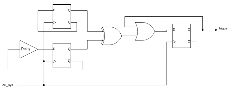
The idea behind these detectors is straightforward: the output of two D-latches is XORed to detect differences. If a glitch is injected, it may flip the state of only one of the latches, immediately triggering the detector. To detect glitches that could flip both latches, a delay is inserted in the feedback path of one of the latches. If the glitch flips both D-latches simultaneously, the delayed feedback would force the latches to take on different values on the next clock cycle and the detector would be triggered.
Each of the four detectors can be independently configured via the GLITCH_DETECTOR.SENSITIVITY register or the OTP fuse CRIT1.GLITCH_DETECTOR_SENS. There are four sensitivity levels available, allowing fine-tuned detection based on the expected operating environment.
When a glitch is detected, the GLITCH_DETECTOR.TRIG_STATUS register indicates which of the detectors were triggered. If the glitch detectors are armed – either by writing to the GLITCH_DETECTOR.ARM register or by programming the OTP fuse CRIT1.GLITCH_DETECTOR_ENABLE – a reset is asserted automatically upon detection. In such cases, the HAD_GLITCH_DETECT bit in the POWMAN.CHIP_RESET register is set, indicating that the last reset was caused by the glitch detector.
Interestingly, it’s possible to monitor the output of the glitch detectors without triggering a reset – a feature that proves very useful when characterizing the detectors and tuning glitch parameters during testing.
The fact that the chip includes only four glitch detectors raises an important question: how resilient is this design against localized fault injection? It’s clear that a focused laser fault injection (L-FI) attack should bypass these detectors. This has been demonstrated by the winner of the Pico2 challenge, Kévin Courdesses, who modified an OpenFlex microscope to inject laser glitches.
But what about more common localized FI methods, like electromagnetic fault injection (EMFI) or body-bias injection (BBI)? That’s something we’ll explore in a future post, but Thomas Roth has already demonstrated that such an attack is feasible.
Characterizing the CPU with crowbar glitching
The first step in our evaluation was to assess the CPU’s sensitivity to voltage glitches. For this initial fault injection (FI) campaign, we disabled all glitch detectors – setting the sensitivity level to 0 and not arming them – in order to observe the CPU’s raw behavior without any interference from built-in protections and countermeasures.
For the glitching technique, we opted for crowbar switching, one of the most widely used methods in voltage fault injection. Its popularity stems largely from the simplicity and affordability of the hardware required. However, crowbar switching also offers technical advantages over other voltage glitching methods, which we’ll discuss later. In future posts, we’ll also cover results obtained using a DAC to generate voltage glitches and compare the two approaches in terms of effectiveness and control.
To inject the glitches, we used a tool called Glitch.IO. This tool is an in-house development based on the Raspberry Pi Pico, like many other glitchers, but with several unique features not previously seen in similar tools. Some of these unique features will be introduced throughout this series of posts. The Glitch.IO will be released as open hardware soon during Black Hat USA 2025.

Modifying the Pico2 board
Before performing glitching experiments on the Raspberry Pi Pico 2, we first needed to modify the board to isolate the CPU power plane and remove its associated capacitance.
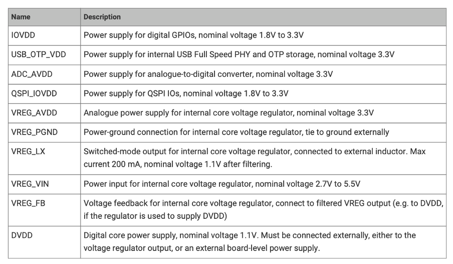
According to the datasheet (see Figure 3), the RP2350 features five power supply domains. However, only one is relevant for our purposes: DVDD – the 1.1V rail that powers the CPU core. This is the supply line where we’ll be injecting our glitches. The remaining power supplies operate at 3.3V and are not initially of interest for this stage of testing.
Note: Aedan Cullen – the third winner of the Pico2 challenge – found that the USB_OTP_VDD power rails is also interesting for glitching. I recommend his presentation at the 38C3.
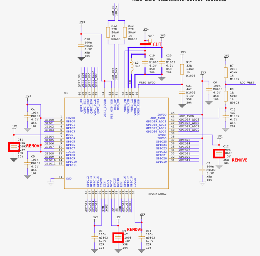
To reduce the bill of materials (BOM) and facilitate the PCB design, the RP2350 chip has an integrated Switched-Mode Power Supply (SMPS ) that can generate the 1.1V from the 3.3V rail.
Referring to the Raspberry Pi Pico 2 schematics (available as an annex in the datasheet), we identified the decoupling capacitors on the DVDD power plane: C9, C11, and C12. These were removed to reduce the capacitance on the DVDD line, making the PCB more susceptible to glitches. Additionally, since we plan to perform DAC-based glitching and supply custom voltage profiles to the core, we had to isolate the DVDD pins from the SMPS output. To do this, we cut the trace connecting the 1.1V line to VREG_FB, effectively decoupling the internal regulator. We then supplied power directly to the DVDD rail using test point TP7 and an external power supply.
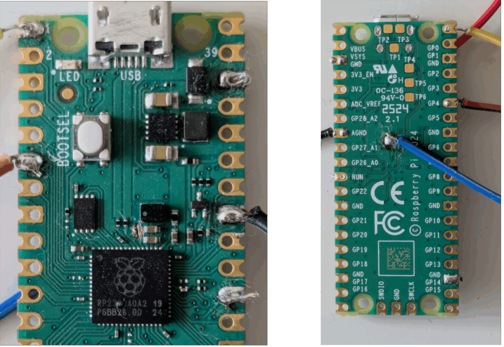
Figure 4 shows all of the modifications done in the schematic, and Figure 5 shows those modifications on the PCB.
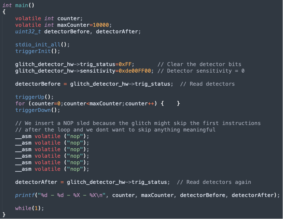
The test application
To characterize the target, we developed a standard “for loop” test application, shown in Figure 6, that will run on the Raspberry Pico 2. Before entering the loop, the glitch detectors are configured. After the loop is completed, the application prints the status of the detectors.
The goal of this fault injection (FI) campaign is to determine the optimal glitch parameters that can disrupt the execution of the loop without triggering the glitch detectors.
The glitch application
The glitching tool must run an application responsible for four key tasks:
1. Preparing the target device for glitching
2. Waiting for a trigger
3. Injecting the glitch
4. Evaluating the target’s response and the glitch’s effects
The Glitch.IO SDK simplifies the development of such applications. It provides a collection of modular classes designed to abstract and streamline the glitching process:
- Glitchers: Implement different glitching techniques, such as crowbar, DAC-generated glitches, clock glitches, reset glitches, and MUX switching.
- Triggers: Define how glitches are synchronized, supporting a variety of trigger sources (e.g., GPIO rise/fall, reset lines, UART RX/TX).
- Protocols: Implement generic communication protocols like SWD, JTAG, etc.
- Targets: Define the specific attack or test logic – for example, attacking secure boot, bypassing debug protections, or characterizing glitch sensitivity.
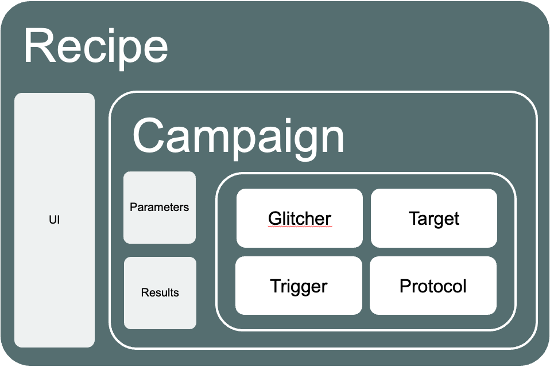
These components are instantiated and combined to form a “recipe” – an application that implements a specific attack on a specific device. Figure 7 represents the software architecture of a Glitch.IO application, and the following code shows the recipe used to characterize the Raspberry Pico 2.
void initializeParameters(unordered_map<string, Parameter*> ¶meters) {
parameters["DELAY"] = new RandomParameter(1000,1100);
parameters["GLITCHVOLTAGE"] = new RandomParameter(1400,1980);
parameters["LENGTH"] = new RandomParameter(1,45);
parameters["NORMALVOLTAGE"] = new FixedParameter(1400); //1.1V
}
int main() {
unordered_map<string, Parameter*> parameters;
Config config;
io_init();
stdio_init_all();
io_uartInit(115200, 8, UART_PARITY_NONE, 1);
initializeParameters(parameters);
initializeConfig(config);
SingleCrowbar glitcher;
RisingGpioTrigger trigger;
StandardLoopCountermeasures target(10000);
Campaign campaign("Pico2 loop characterization with countermeasures",100000);
UI ui;
campaign.setParameters(parameters);
campaign.setConfig(config);
campaign.setGlitcher(&glitcher);
campaign.setTarget(&target);
campaign.setTrigger(&trigger);
campaign.setTimeout(100000); // 100ms
ui.setCampaign(&campaign);
ui.loop();
} In this recipe, glitch parameters and their variation strategies are defined in initializeParameters(). In main(), we instantiate and wire together the glitcher, trigger, and target components.
The Glitch.IO SDK also includes example recipes for common FI attacks against popular MCUs from vendors like NXP and ST – making it easy to get started with real-world targets.
The FI campaign
The glitch detectors in the RP2350 can be configured at four different sensitivity levels. For each level, we ran a series of FI campaigns: starting with broad glitch parameter sweeps and then progressively narrowing them down in an attempt to maximize the success rate – defined as glitches that disrupt execution without being detected.
Throughout the campaigns, we logged two key outcomes:
- Whether the glitch was successful (i.e., it altered the behavior of the for loop).
- Which glitch detectors, if any, were triggered.
All tests were performed using an external 1.1V power supply, and the chip was reset after each glitch attempt to ensure a consistent starting state.
During testing, the injected glitches produced a variety of observable effects. We classified the results into the following categories:
- Normal: The glitch had no observable effect on chip behavior.
- Reset: The glitch caused a system crash or full reset.
- Success: The loop counter was altered, but no glitch detectors were triggered.
- Detected 1–4: The loop counter was altered, and one to four glitch detectors were triggered, respectively.
- Unknown: The device printed unexpected characters, suggesting some level of corruption.
- Error: Any other unclassified or abnormal behavior.
The following sections summarize the results of the fault injection characterization campaigns, organized by glitch detector sensitivity level.
Sensitivity Level 0 (glitch_detector_hw->sensitivity=0xDE00FF00)
The following sections summarize the results of the fault injection characterization campaigns, organized by glitch detector sensitivity level.
Sensitivity Level 0 (glitch_detector_hw->sensitivity=0xDE00FF00)
At this lowest sensitivity level, the glitch detectors are effectively disabled – they seemed to not be functional and could not be triggered. This allowed us to focus purely on the CPU’s sensitivity to glitches without interference from detection mechanisms.
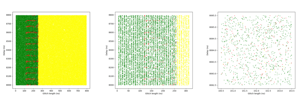
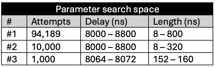
We conducted three separate FI campaigns at this level, progressively narrowing the glitch parameters (e.g., delay and length) to identify the most effective combinations.
Figure 8 shows the plots of the glitch results. A clear boundary is visible between the green and yellow zones: this is where the glitch becomes too long or powerful, consistently crashing the target. The red points appear along this boundary, but only at specific delay values – those that align precisely with the execution of the instruction that when glitched breaks the loop. This correlation provides strong insight into the CPU’s timing sensitivity and the ideal glitch injection window. The highest success rate achieved was almost 14%.
The following tables summarize the results for these campaigns:
LEVEL 0 (glitch_detector_hw->sensitivity=0xDE00FF00)
Sensitivity Level 1 (glitch_detector_hw->sensitivity=0xDE00AA55)
At this sensitivity level, the glitch detectors were still unable to detect any of the injected glitches. The results were largely indistinguishable from those observed at Sensitivity Level 0.
Due to the lack of significant behavioral differences, only a single short campaign was conducted at this level to confirm the similarity. No glitches were detected, and successful fault injections continued to occur under the same timing and voltage conditions as before.
The following tables summarize the results for this campaign:
LEVEL 1 (glitch_detector_hw->sensitivity=0xDE00AA55)
Sensitivity Level 2 (glitch_detector_hw->sensitivity=0xDE0055AA)
This is the first sensitivity level at which the glitch detectors were successfully triggered by our fault injections. However, it was still relatively easy to bypass the detectors under certain conditions.
In the plot shown in Figure 10, additional colors indicate the number of detectors triggered during successful glitches – that is, glitches that broke the loop logic but:
- Blue: 1 detector was triggered
- Magenta: 2 detectors were triggered
- Cyan: 3 detectors were triggered
- Purple: All 4 detectors were triggered
To improve clarity, a second version of the plot is included, where green (normal glitches) and yellow (reset events) have been removed, making it easier to focus on detection behavior.
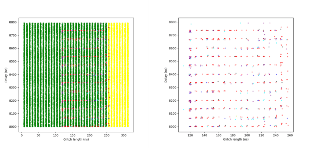
A success rate of nearly 7% was achieved in this campaign – relatively high, considering this was the third level of sensitivity. These results suggest that while detection is now functional, the protection can still be bypassed with a well-timed and well-parameterized glitch.
The following tables summarize the different campaigns conducted at this sensitivity level and their respective outcomes.
LEVEL 2 (glitch_detector_hw->sensitivity=0xDE0055AA)
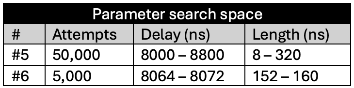
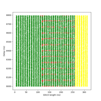
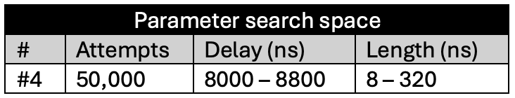
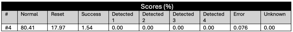
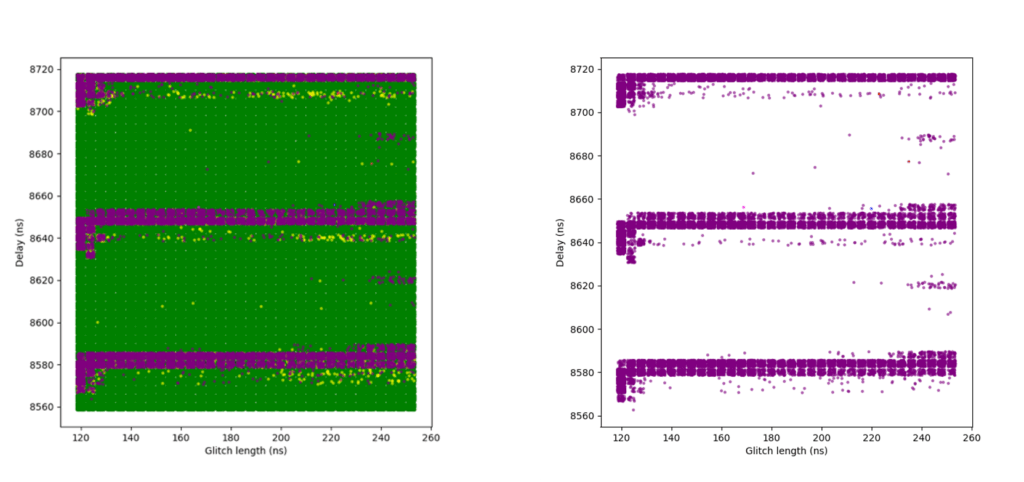
Sensitivity Level 3 (glitch_detector_hw->sensitivity=0xDE0000FF)
At this highest sensitivity level, the glitch detectors become very effective. Although we were still able to achieve some successful glitches, the success rate dropped significantly.
An initial campaign using broader parameters resulted in a small number of successful glitches. A second campaign attempted to narrow the parameter range based on what had worked at Sensitivity Level 2 but yielded no successful results. In hindsight, this was likely due to insufficient glitch attempts.
A third and final campaign expanded the narrowed parameter range slightly and achieved a modestly improved success rate. However, even then the rate was only about 0.0002%, indicating that the detectors are highly effective at this level.
One interesting observation is that while at Sensitivity Level 2, many glitches triggered only one, two, or three detectors, at Sensitivity Level 3, glitches almost always triggered all four detectors.
The following plots show the two campaigns with broader parameters. In the right-hand plots, green and yellow dots are removed to better highlight successful red points.
Additional campaigns (not included in this article) attempted to further refine parameters around previously successful glitches, but did not yield any improvement in the success rate.
The following tables summarize the results for the three campaigns conducted at this sensitivity level.
LEVEL 3 (glitch_detector_hw->sensitivity=0xDE0000FF)
Conclusions
Our experiments demonstrate that the RP2350’s glitch detectors are highly effective – but only when configured at the highest sensitivity level. At Sensitivity Levels 0 and 1, the detectors provided no meaningful protection. Sensitivity Level 2 reduced the success rate significantly, but not enough to prevent a fault injection (FI) attack (almost a 7% success rate).
Even at Sensitivity Level 3, it was still possible to glitch the RP2350, albeit with a very low success rate of approximately 0.00016% – or roughly one successful glitch every 625,000 attempts. Given that our setup could inject glitches at around 30 attempts per second, this translated to an average attack time of under six hours to achieve a successful result.
However, it’s crucial to place these results in context to properly evaluate the real-world risk of using the RP2350 in a security-critical application.
All experiments were conducted under ideal lab conditions:
- Full control over the target
- Precise and reliable trigger signals
- Fast reset cycle
- A test application that executes the vulnerable instruction repeatedly, every few clock cycles
These ideal conditions greatly increased our odds of success. In contrast, a real-world attack would face substantial challenges:
- Limited or no access to CPU internals
- Unreliable or noisy trigger sources
- Potentially long and variable reset/restart times
- Application code that executes sensitive operations infrequently or unpredictably
Introducing software countermeasures – such as instruction-level redundancy or random delays – would further reduce the success rate, often requiring multiple or perfectly timed glitches. Under such constraints, an attacker may require several months to mount a successful attack using crowbar-based glitching alone.
In future articles, we’ll explore whether the same conclusions hold for other glitching techniques, such as DAC-generated glitches or electromagnetic fault injection (EMFI).
Note: The winners of the Raspberry Pi Pico 2 challenge have shown that crowbar glitching the RP2350 can be much easier under specific conditions:
– Aedan Cullen successfully attacked the USB_OTP_VDD rail – a power domain not monitored by the glitch detectors.
– Marius Muench targeted the main VCC rail. However, as of this writing, no public information has been released about his glitching method or achieved success rate.