
This is Part 3 of a 3-Part series. You can find Part 1 here and Part 2 here.
Introduction
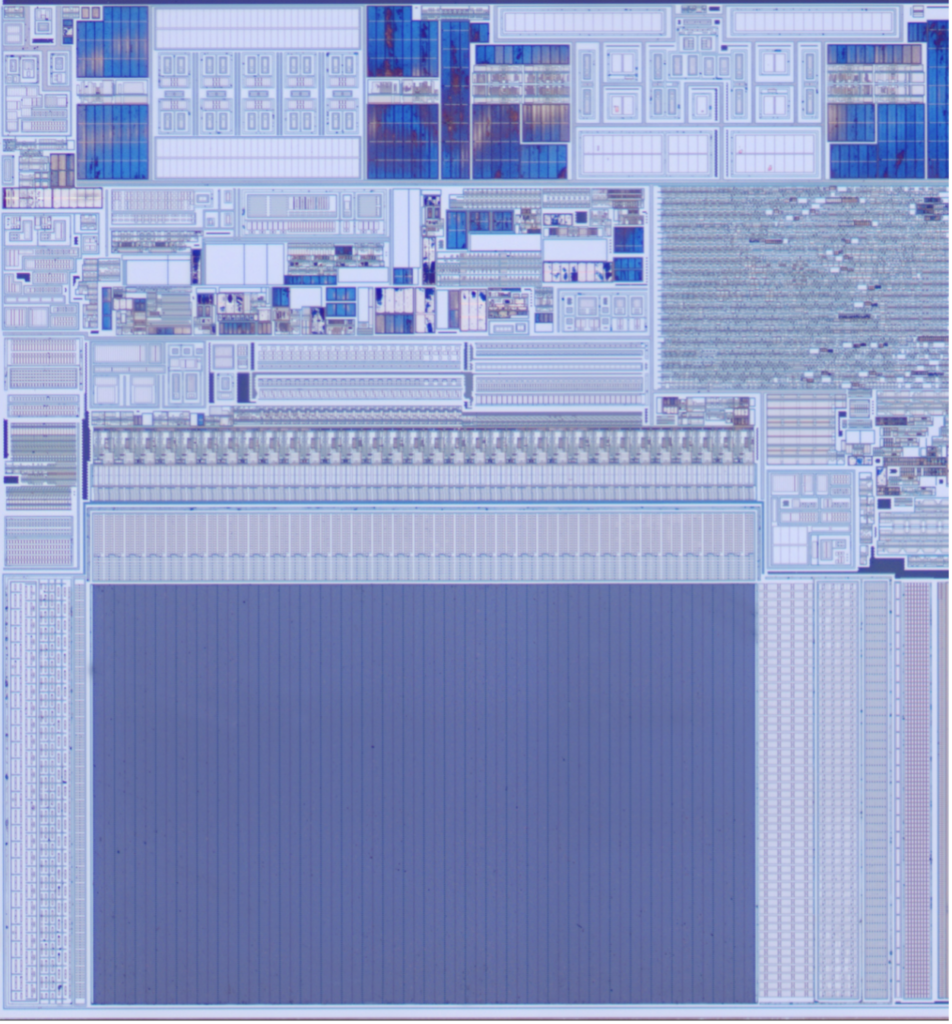
In this post, we continue our deep dive comparison of the security processors used on a consumer product and an unlicensed clone. Our focus here will be identifying and characterizing memory arrays.
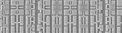
Given a suitably deprocessed sample, memories can often be recognized as such under low magnification because of their smooth, regular appearance with distinct row/address decode logic on the perimeter, as compared to analog circuitry (which contains many large elements, such as capacitors and inductors) or autorouted digital logic (fine-grained, irregular structure).
Identifying memories and classifying them as to type, allows the analyst to determine which ones may contain data relevant to system security and assess the difficulty and complexity of extracting their content.
OEM Component
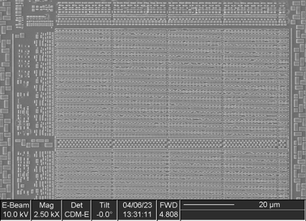
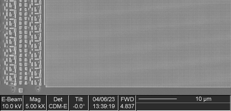
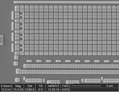
Initial low-magnification imaging of the OEM secure element identified 13 structures with a uniform, regular appearance consistent with memory.
Higher magnification imaging resulted in three of these structures being reclassified as non-memory (two as logic and one as analog), leaving 10 actual memories.
Of the remaining 10 memories, five distinct bit cell structures were identified:
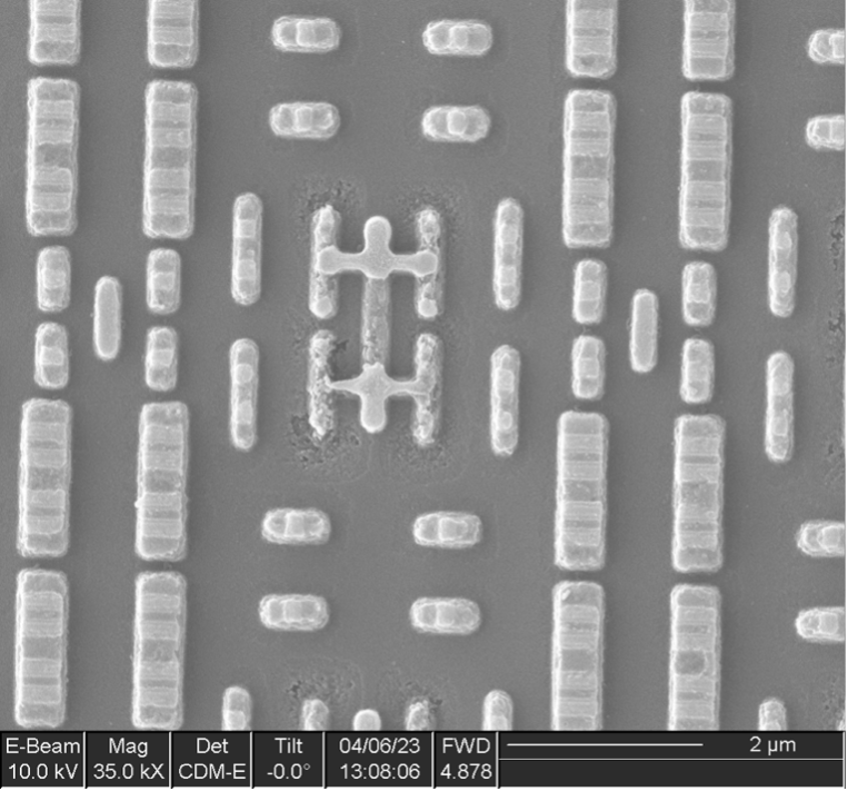
- Single-port (6T) SRAM
- Dual-port (8T) SRAM
- Mask ROM
- 3T antifuse
- Floating gate NOR flash
Single-port SRAM
13 instances of this IP were found in various sized arrays, with capacities ranging from 20 bits x 8 rows to 130 bits x 128 rows.
Some of these memories include extra columns, which appear to be intended as spares for remapping bad columns. This is a common practice in the semiconductor industry to improve yield: memories typically cover a significant fraction of the die surface and thus are responsible for a large fraction of manufacturing defects. If the device can remain operable despite a defect in a memory array, the overall yield of usable chips will be higher.
Dual-port SRAM
Six instances of this IP were found, each containing 320 bit cells (40 bytes).
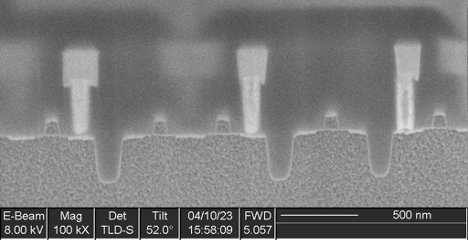
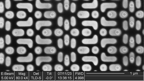
Mask ROM
Two instances of this IP were found, with capacities of 256 Kbits and 320 Kbits respectively. No data was visible in a substrate view of the array.
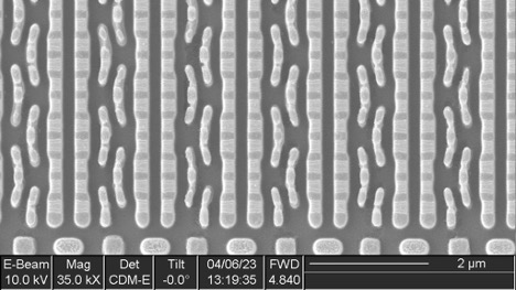
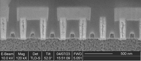
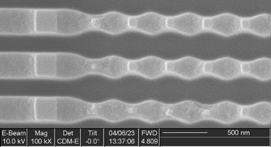
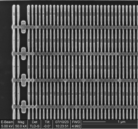
A cross section (Figure 7) showed irregular metal 1 patterns as well as contacts that did not go to any wires on metal 1, strongly suggesting this was a metal 1 programmed ROM. A plan view of metal 1 (Figure 8) confirms this. The metal 1 pattern also shows that the transistors are connected in series strings of 8 bits (with each transistor in the string either shorted by metal or not, in order to encode a logic 0 or 1 value), completing the classification of this memory as a metal 1 programmed NAND ROM.
IOActive successfully extracted the contents of both ROMs and determined that they were encrypted. Further reverse engineering would be necessary to locate the decryption circuitry in order to make use of the dumps.
Antifuse
Five instances of this IP were found, four with a capacity of 4 rows x 32 bits (128 bits) and one with a capacity of 32 rows x 64 bits (2048 bits).
The bit cells consist of three transistors (two in series and one separate) and likely function by gate dielectric breakdown: during programming, high voltage applied between a MOSFET gate and the channel causes the dielectric to rupture, creating a short circuit between the drain and gate terminals.
Antifuse memory is one-time programmable and is expensive due to the very low density (significantly larger bit cell compared to flash or ROM); however, it offers some additional security because the ruptured dielectric is too thin to see in a top-down view of the array, rendering it difficult to extract the contents of the bit cells. It is also commonly used for small memories when the complexity and re-programmability of flash memory is unnecessary, such as for storing trim values for analog blocks or remapping data for repairing manufacturing defects in SRAM arrays.
Flash
A single instance of this IP was found, with a capacity of 1520 Kbits.
This memory uses floating-gate bit cells connected in a NOR topology, as is common for embedded flash memories on microcontrollers.
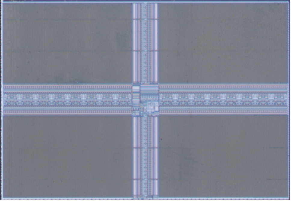
Clone Component
Floorplan Overview
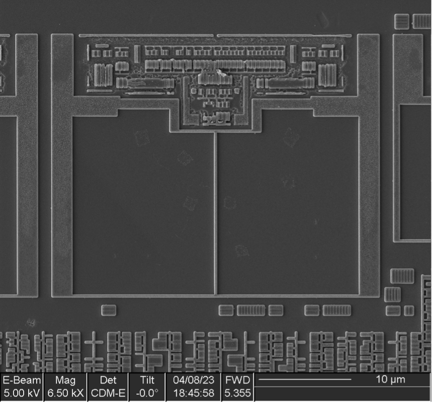
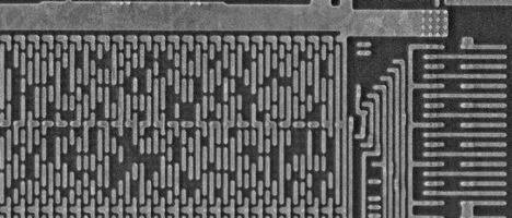
The secure element from the clone device contains three obvious memories, located at the top right, bottom left, and bottom right corners.
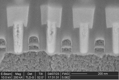
Lower-left Memory
The lower-left memory consists of a bit cell array with addressing logic at the top, left, and right sides. Looking closely, it appears to be part of a larger rectangular block that contains a large region of analog circuitry above the memory, as well as a small amount of digital logic.
This is consistent with the memory being some sort of flash (likely the primary code and data storage for the processor). The large analog block is probably the high voltage generation for the program/erase circuitry, while the small digital block likely controls timing of program/erase operations.
The array appears to be structured as 32 bits (plus 2 dummy or ECC columns) x 64 blocks wide, by 2 bits * 202 rows (likely 192 + 2 dummy features + 8 spare). This gives an estimated usable array capacity of 786432 bits (98304 bytes, 96kB).
A cross section was taken, which did not show floating gates (as compared to the OEM component). This suggests that this component is likely using a SONOS bit cell or similar charge-trapping technology.
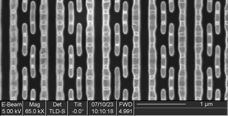
Lower-right Memory
The lower-right memory consists of two identical blocks side-by-side, mirrored left-to-right. Each block consists of 128 columns x 64 cells x 3 blocks high, for a total capacity of 49152 bits (6144 bits, 6 kB).
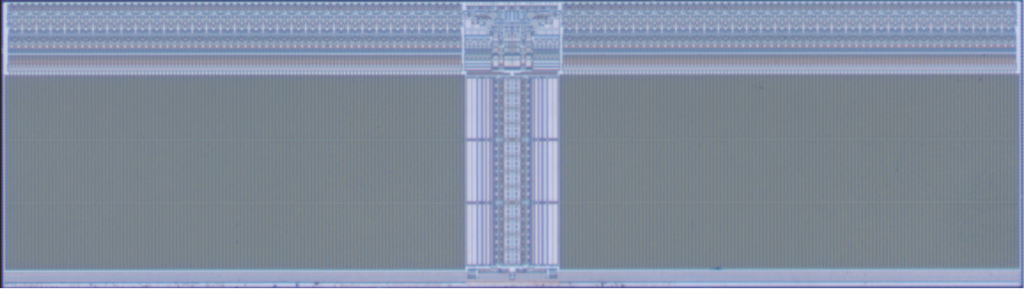
At higher magnification, we can see that the individual bit cells consist of eight transistors, indicative of dual-port SRAM—perhaps some sort of cache or register file.
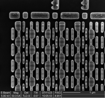
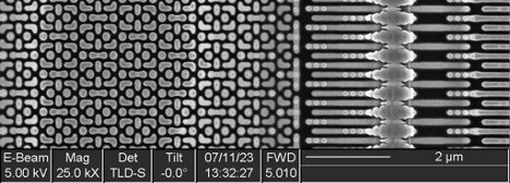
Upper-right Memory
The upper – right memory consists of a 2 x 2 grid of identical tiles, each 128 columns x 160 rows (total capacity 81920 bits/10240 bytes/10 kB).
Upon closer inspection, the bit cell consists of six transistors arranged in a classic single-port SRAM structure.
Concluding Remarks
The OEM component contains two more memory types (mask ROM and antifuse) than the clone component. It has double the flash memory and nearly triple the persistent storage (combined mask ROM and flash) capacity of the clone, but slightly less SRAM.
Overall, the memory technology of the clone component is significantly simpler and lower cost.
Overall Conclusions
OEMs secure their accessory markets for the following reasons:
- To ensure an optimal user experience for their customers
- To maintain the integrity of their platform
- To secure their customers’ personal data
- To secure revenue from accessory sales
OEMs routinely use security chips to protect their platforms and accessories; cost is an issue for OEMs when securing their platforms, which potentially can lead to their security being compromised.
Third-party solution providers, on the other hand:
- Invest in their own labs and expertise to extract the IP necessary to make compatible solutions
- Employ varied attack vectors with barriers of entry ranging from non-invasive toolsets at a cost of $1,000 up, to an invasive, transistor-level Silicon Lab at a cost of several million dollars
- Often also incorporate a security chip to secure their own solutions, and to in turn lock out their competitors
- Aim to hack the platform and have the third-party accessory market to themselves for as long as possible