
This is Part 2 of a 3-Part series. You can find Part 1 here.
Introduction
In this post, we continue our deep dive comparison of the security processors used on a consumer product and an unlicensed clone. Our focus here will be comparing manufacturing process technology.
We already know the sizes of both dies, so given the gate density (which can be roughly estimated from the technology node or measured directly by locating and measuring a 2-input NAND gate) it’s possible to get a rough estimate for gate count. This, as well as the number of metal layers, can be used as metrics for overall device complexity and thus difficulty of reverse engineering.
For a more accurate view of device complexity, we can perform some preliminary floorplan analysis of each device and estimate the portions of die area occupied by:
- Analog logic (generally uninteresting)
- Digital logic (useful for gate count estimates)
- RAM (generally uninteresting aside from estimating total bit capacity)
- ROM/flash (allows estimating capacity and, potentially, difficulty of extraction)
OEM Component
We’ll start with the OEM secure element and take a few cross sections using our dual-beam scanning electron microscope/focused ion beam (SEM/FIB). This instrument provides imaging, material removal, and material deposition capabilities at the nanoscale.
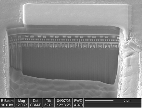
To cross section a device, the analyst begins by using deposition gases to create a protective metal cap over the top of the region of interest. This protects the top surface from damage or contamination during the sectioning process. This is then followed by using the ion beam to make a rough cut a short distance away from the region of interest, then a finer cut to the exact location. The sample can then be imaged using the electron beam.
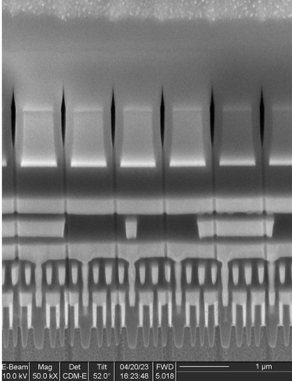
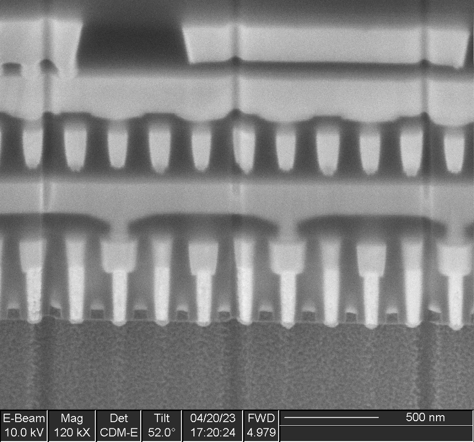
Figure 1 shows a large rectangular hole cut into the specimen, with the platinum cap at top center protecting the surface. Looking at the cut face, many layers of the device are visible. Upon closer inspection (Figure 2), we can see that this device has four copper interconnect layers followed by a fifth layer of aluminum.
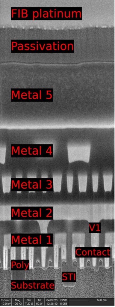
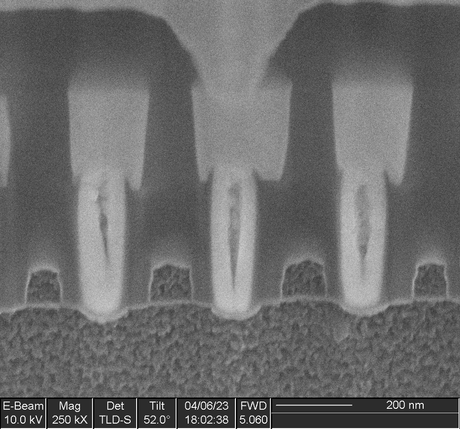
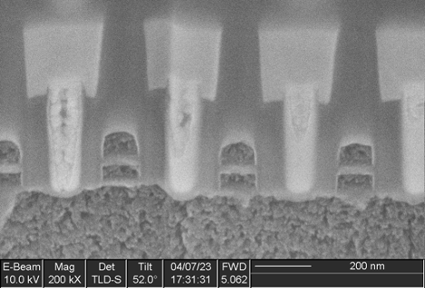
At higher magnification (Figure 3), we can clearly see individual transistors. The silicon substrate of the device (bottom) has been etched to enhance contrast, giving it a rough appearance. The polysilicon transistor gates, seen end-on, appear as squares sitting on the substrate. The bright white pillars between the gates are tungsten contacts, connecting the source and drain terminals of each transistor to the copper interconnect above.
Based on measurements of the gates, we conclude that this device is made on a 90 nm technology:
- Contacted gate pitch: 282 nm
- M1 pitch: 277 nm
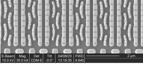
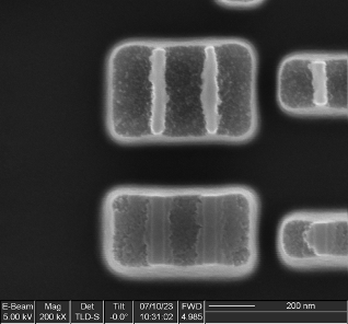
- 6T SRAM bit cell (Figure 4): 1470 x 660 nm (0.97 µm2)
We can also use cross sections to distinguish between various types of memory. Figure 5 is a cross section of one of the memory arrays of the OEM device, showing a distinctive double-layered structure instead of the single polysilicon gates seen in Figure 3. This is a “floating gate” nonvolatile memory element; the upper control gate is energized to select the cell while the lower floating gate stores charge, representing a single bit of memory data.
The presence of metal contacts at both sides of each floating gate transistor (rather than at either end of a string of many bits) allows us to complete the classification of this memory as NOR flash, rather than NAND.
The overall device is approximately 2400 x 1425 µm (3.42 mm2), broken down as:
- 67% (2.29 mm2): memories and analog IP blocks
- 33% (1.13 mm2): standard cell digital logic
Multiplying the logic area by an average of published cell library density figures for the 90nm node results in an estimated 475K gates of digital logic (assuming 100% density) for the OEM security processor. The actual gate count will be less than this estimate as there are some dummy/filler cells in less dense areas of the device.
Clone Component
Performing a similar analysis on the clone secure element, we see five copper and one aluminum metal layers (Figure 6).
Interestingly, the clone secure element is made on a more modern process node than the OEM component:
- Contacted gate pitch: 225 nm
- Minimum poly pitch: 158 nm
- SRAM bit cell: 950 x 465 nm (0.45 µm2)
The transistor gates appear to still be polysilicon rather than metal.
These values are in-between those reported for the 65 nm and 45 nm nodes, suggesting this device is made on a 55 nm technology. The lack of metal gates (which many foundries began using at the 45 nm node) further reinforces this conclusion.
The overall device is approximately 1190 x 1150 µm (1.36 mm2), broken down as:
- 37% (0.50 mm2): memories
- 27% (0.36 mm2): analog blocks and bond pads
- 31% (0.42 mm2): standard cell digital logic
- 5% (0.07 mm2): filler cells, seal ring, and other non-functional areas
Given the roughly 0.42 mm2 of logic and measured NAND2 cell size of 717 x 1280 nm (0.92 µm2 or 1.08M gates/mm2 at 100% utilization), we estimate a total gate count of no more than 450K—slightly smaller than the OEM secure element. The actual number is likely quite a bit less than this, as a significant percentage (higher than on the OEM part) of the logic area is occupied by dummy/filler cells.
In part 3, we continue our deep dive comparison of the security processors used on a consumer product and an unlicensed clone. There we will focus on identifying and characterizing the memory arrays.